Module 5.4
JK Flip-flops
- After studying this section, you should be able to:
- Understand JK Flip-flop circuits and can:
- • Describe typical applications for JK flip-flops.
- • Recognize standard circuit symbols for JK flip-flops.
- • Recognize JK Flip-flop integrated circuits.
- • Describe alternative forms of JK flip-flops.
- Understand timing diagrams to explain the operation of JK flip-flops.
- Use software to simulate JK flip-flops.
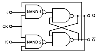
Fig.5.4.1 Basic JK Flip-flop Circuit
A Universal Programmable Flip-flop
The JK Flip-flop is also called a programmable flip-flop because, using its inputs, J, K, S and R, it can be made to mimic the action of any of the other flip-flop types.
Fig. 5.4.1 shows the basic configuration (without S and R inputs) for a JK flip-flop using only four NAND gates. The circuit is similar to the clocked SR flip-flop shown in Fig. 5.2.7, (Digital Electronics Module 5.2) but in Fig. 5.4.1, it can be seen that although the clock input is the same as in the clocked SR flip-flop, gate NAND 1 in Fig. 5.4.1 is now a three input gate and the set input (S) been replaced by an input labeled J, and the third input provides feedback from the Q output.
On NAND 2 the reset input (R) of Fig 5.2.7 has been replaced by input K and there is an additional feedback connection from Q. The purpose of this feedback is to eliminate the indeterminate state that occurred on the SR flip-flop when both inputs were made logic 0 at the same time.
Operation
As a starting point, assume that both J and K are at logic 1 and the outputs Q = 0 and Q = 1, this will cause NAND 1 to be enabled, as it has logic 1 on two (J and Q) of its three inputs, requiring only a logic 1 on its clock input to change its output state to logic 0. At the same time, NAND 2 is disabled, because it only has one of its inputs (K) at logic 1, its feedback input is at logic 0 because of the feedback from Q.
On the arrival of a clock pulse, the output of NAND 1 therefore becomes logic 0, and causes the flip-flop to change state so that Q = 1 and Q = 0. This action enables NAND 2 and disables NAND 1.
As this change of state at the outputs occurs however, there is a problem. If the clock pulse is still high, or in its thold period when the flip-flop changes state, the output of NAND 2 will instantly go to logic 0 and the flip-flop will reset back to its original state. This can then set up a situation where the flip-flop will rapidly oscillate between its two states.
These problems caused by the output data ‘racing’ round the feedback lines from output to input before the end of the clock pulse are known as RACE HAZARDS and of course must be avoided. This can be done however, by using a more complex version of the circuit.
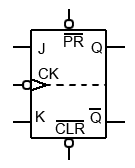
Fig. 5.4.2 JK Master-Slave Flip-Flop Symbol
The JK Master Slave Flip-flop.
As well as minimising the race hazards problem, this type of flip-flop can also function as an SR, a clocked SR, a D type, or a Toggle flip-flop. The ‘master slave’ terminology refers to the device having two separate flip-flop stages, isolating the input from the output. As well as reducing the race hazards problem, it also has a further advantage over the simpler SR types, as its J and K inputs can be any value without causing any indeterminate state.
A typical circuit symbol is shown in Fig 5.4.2, and Table 5.4.1 shows how different logic combinations applied to the J and K inputs change the way the JK flip-flop responds to the application of a clock pulse on the CK input.
JK Synchronous Inputs
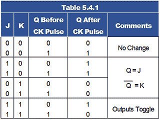
• When J and K are both 0 the flip-flop is inhibited, Q is the same after the CK pulse as it was before; there is no change at the output.
• If J and K are at different logic levels, then after the CK pulse, Q and Q will take up the same states as J and K. For example, if J = 1 and K = 0, then on the trailing (negative going) edge of a clock pulse, the Q output will be set to 1, and if K = 1 and J = 0 then the Q output is reset to logic 0 on the trailing edge of a clock pulse, effectively mimicking the D type master slave flip-flop by replacing the D input with J.
• If logic 1 is applied to both J and K, the output toggles at the trailing edge of each clock pulse, just like a toggle flip-flop.
The JK flip-flop can therefore be called a ‘programmable flip-flop’ because of the way its action can be programmed by the states of J and K.
Each of the above actions are synchronised with the clock pulse, data being taken into the master flip-flop at the rising edge of the clock pulse, and output from the slave flip-flop appears at the falling edge of the clock pulse.
Note: Although the above describes the action of a master slave JK flip-flop, there are also positive edge and negative edge triggered versions available.
Asynchronous Inputs
Asynchronous inputs, which act independently of the clock pulse, are also provided by the active low inputs PR and CLR. These act as (usually active low) SET and RESET inputs respectively, and as they act independently of the clock input, they give the same facilities as a simple SR flip-flop. As with the SR flip-flop, in this mode some external method is needed to ensure that these two inputs cannot both be active at the same time, as this would make both Q and Q logic 1.
JK Master-Slave Operation
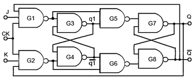
A theoretical schematic circuit diagram of a level triggered JK master slave flip-flop is shown in Fig 5.4.3. Gates G1 and G2 form a similar function to the input gates in the basic JK flip-flop shown in Fig. 5.4.1, with three inputs to allow for feedback connections from Q and Q.
Gates G3 and G4 form the master flip-flop and gates G7 and G8 form the slave flip-flop. Two further gates, G5 and G6, are included between the master and slave to transfer data from the master to the slave. The way this transfer happens is that the output of the master flip-flop is delayed for the duration of the clock pulse, by storing it, temporarily in the master flip-flop, whilst the CK pulse is high. The operation (in toggle mode) is as follows:
Loading the Master Flip-flop
With J and K both at logic 1 (the toggle mode setting), suppose that Q = 0 and Q = 1, gate G2 will be disabled as, although there are two logic 1 states on its J and CK inputs, the feedback (bottom) input of G2 will be at logic 0 due to the feedback from Q.
G1 however has a logic 1 fed back from Q, which ensures that gate G1 is enabled, as all three of its inputs are now logic 1. G1 output will therefore be at logic 0 (NAND gate rules), which will cause the master flip-flop (G3 and G4) to set its q1 output to logic 1, and its q1 output to logic 0.
During the time the CK input remains at logic 1, q1 and q1 will remain at q1 = 1 and q1 = 0, but the transfer gates G5 and G6 are inhibited because for example, if Q is currently at logic 0 and Q is at logic 1, gate G1 will have all three of its inputs at logic 1, and so its output will be 0. Because G1 output is also the active low SET input of G3, as the CK pulse went to logic 1, G3 output went to logic 0, setting the master flip-flop output q1 to logic 1.
Controlling the Transfer Gates
The logic 0 on G1 output will cause transfer gate G5 to be disabled, and combined with the logic 1 at q1 this will cause G5 output to remain at logic 1 for the duration of the CK pulse. The input to G6 from G2 output however will be at logic 1, but as q1 will now be at logic 0, transfer gate G6 will also be disabled, making its output logic 0. The data at the outputs q1 and q1 will therefore not be passed to the slave flip-flop for the duration of the clock pulse.
The Clock Pulse Falling Edge
Once the clock input goes low however, logic 0 is applied to the clock inputs of gates G1 and G2. The output of G1 now returns to logic 1, making both inputs to gate G5 logic 1, and causing its output to fall to logic 0. As q1 is still at logic 0, gate G6 is still disabled, and so the output of G6 is at logic 1.
The Slave Flip-flop
With the output of Gate G5 at logic 0 and G6 output at logic 1, gates G7 and G8, which form a low activated SR flip-flop is set, and so Q becomes logic 1 and Q becomes logic 0.
The output conditions are now inverted, and this change is fed back to the input gates G1 and G2. However these are now both disabled because the clock input is already low, so the master flip-flop is not affected.
The arrival of the rising edge of the next clock pulse then allows the new logic levels at Q and Q into the feedback inputs to gates G1 and G2 to be fed into the master flip-flop as before, but this time Q is at logic 1, so it is gate G2 that will be enabled at the rising edge of the clock pulse.
Now, as the clock pulse goes to logic 1 the master flip-flop will be reset, q1 will go to logic 0 and at the falling edge of the clock pulse the transfer gates will pass the data to the slave flip flop setting Q back to logic 0, so the Q and Q outputs toggle once more.
JK Flip-flop Circuit Variations
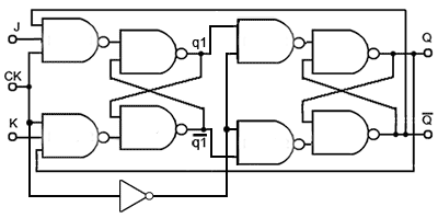
Although the standard JK flip-flop circuit shown in Fig. 5.4.3 works, the inclusion of the transfer gates limits the circuit‘s operation to level triggering. However Fig 5.4.4 illustrates a different method of transferring data from the master to the slave flip-flop. Instead of the transfer gates G5 and G6 used in Fig. 5.4.3, Fig. 5.4.4 uses a NOT gate to invert the positive going CK pulse triggering the master flip-flop, producing an inverted version of the clock pulse to trigger the slave flip-flop. with this modification data is clocked into the master flip-flop at the rising edge of the CK input. Any further changes in data at J or K do not now affect the state of the master flip-flop whilst CK is high, because the feedback from Q and Q will always disable which ever of the two input gates could make a change to the master flip flop.
Due to the CK inverter, at the falling edge of the CK pulse, the slave flip-flop now sees a rising edge, and the slave flip-flop accepts the data from q1 and q1 toggling the states of Q and Q. This master slave circuit therefore only accepts data from J and K at the rising edge of CK and outputs it on Q and Q at the falling CK edge.
However, in both Figs. 5.4.3 and 5.4.4 the master and slave flip-flops are both simple level triggered clocked SR flip-flops. Both designs work as predicted for a JK flip-flop, in toggle mode. However, in modes where J and K can change, the master flip-flop in Fig 5.4.3 accepts data from the J and K inputs whenever the CK pulse is high, allowing the master flip-flop outputs to change as long as the CK pulse is high. Therefore it is the data that is present at the instant before the CK falling edge, which is passed to the slave flip-flop. In Fig 5.4.4 the master flip-flop only accepts data at the rising edge of CK, and outputs that data at the falling edge of the CK pulse.
Although the slave flip-flop is also level triggered, it will not change after the clock input has gone low, because its input is taken from the output of the master flip-flop, which will not be accepting changes due to the clock input being low.
JK Flip-flops Using D Type Devices
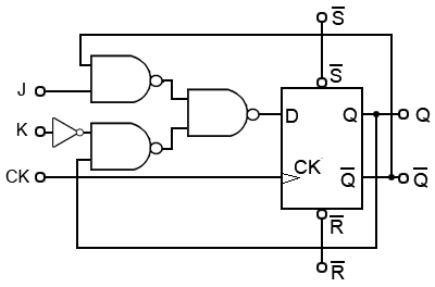
Fig. 5.4.5 shows a positive edge triggered JK flip-flop (not master slave) constructed from a positive edge triggered D Type flip-flop, that uses a modified data select circuit to correctly steer the feedback from Q and Q outputs to the J and K inputs.
This circuit also makes use of the asynchronous SET and RESET inputs of the D Type flip-flop, and because the D Type is edge triggered, this version of a JK flip flop is truly edge (not level) triggered. It is also possible to use a negative edge triggered D Type flip-flop to make a negative edge triggered JK flip-flop by this method.
JK Master Slave Flip-flop Using D Type Flip-flops
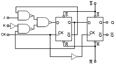
Fig. 5.4.6 shows a JK Master Slave Flip-flop using two positive edge triggered D Type flip-flops and inverting the clock pulse to convert the slave flip-flop to negative edge triggering.
This design therefore, has true edge triggering on both rising and falling edges of the clock pulse, and is immune from any changes in data happening during the high or low level periods of the clock signal (except for any changes or disturbances that may occur during the Tsetup or thold periods close to the clock pulse edges, as described in Sequential Logic Module 5.3).


