Module 4.6
Pulse Width Modulation
- After Studying this section, you should be able to:
- • Understand how timer ICs can be used for PWM.
- • Know basic methods of pulse width control.
- • Apply PWM principles to motor control.
- • Understand back EMF protection for inductive loads.
Using Astables & Monostables for Pulse Width Modulation (PWM)
Monostables are widely used in generating simple time delays, an example of which could be the delay in switching off the courtesy light in a car, some seconds after the ignition switch is turned off. There are many other uses however that also make use of the 555 timer’s versatility.
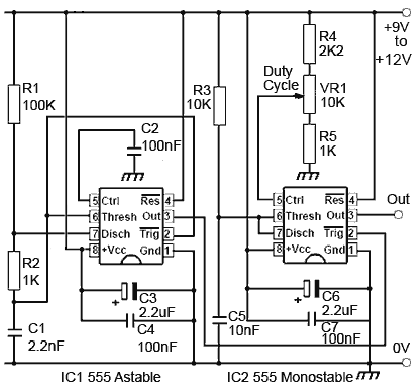
Fig. 4.6.1 Pulse Width Modulation with Astable & Monostable
In the 555 astable examples shown in Oscillator Module 4.4, the control input (pin5) of the 555 was shown to be useful in controlling the duty cycle of the output. However its action also varied the frequency of the astable. This interdependence can be eliminated by using two 555 timers, the first as a constant frequency astable pulse generator, driving the Trigger input of a second 555 used as a monostable, with its delay timing varied by a voltage applied to its control pin. Such circuits can be constructed using either two 555 timer ICs or a single 556 Dual timer, which is really two 555s in a single package.
In the circuit shown in Fig. 4.6.1 the duty cycle can be adjusted without any effect on the output frequency, making the circuit useful as a pulse width modulated motor speed control or LED dimmer.
Operation
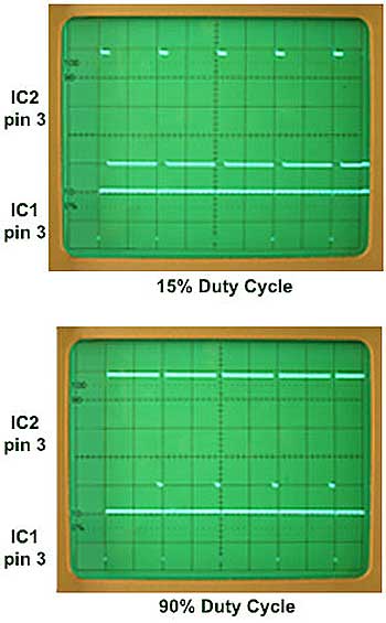
Fig. 4.6.2 Pulse Width Modulation Waveforms
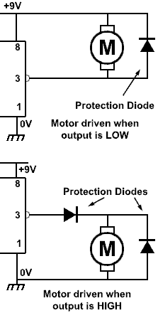
Fig. 4.6.3 Back EMF Protection
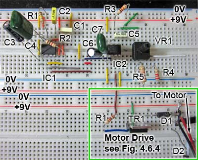
IC1 is a fixed frequency (5kHz) astable producing 2µs negative going pulses repeating every 200µs. Each pulse triggers the monostable IC2, to produce a single output pulse giving a high output, of about 110µs set by the values of the timing components R3 and C5. However this time is altered by the variable voltage applied to pin 5 of IC2 by VR1, allowing the delay period to be varied between about 30 and 180µs, i.e. a duty cycle variable between about 15 and 90% as shown in Fig. 4.6.2, these upper and lower limits being set by the values of R4 and R5 respectively.
The monostable period must always be shorter than the time between the astable pulses to ensure that the monostable is not re-triggered before its time-out, as this would cause output pulses of unpredictable duration.
The narrow negative going pulses produced by IC1 are due to R1 being 100 times greater than R2. The control input (pin 5) of IC1 is not used, and is simply decoupled by C2 to remove any external noise. Both IC1 and IC2 are also externally decoupled by 2.2µF and 100nF capacitors fitted as close to the Vcc and Gnd pins of the ICs as possible. Without this precaution the 555 output can exhibit excessive overshoot at frequencies higher than a few hundred Hz.
Back EMF Protection
The 555 output is capable of sinking or sourcing up to 200mA and so should be quite capable of directly driving small DC motors. However, when connecting inductive loads, such as motors to the 555 output, it is necessary to provide some back e.m.f. protection as shown in Fig. 4.6.3.
For low impedance loads, or if the current drawn by the load is likely to exceed 200mA, a simple emitter follower output driver can be added using a suitable power transistor such as the TIP31A. This will allow output currents up to 3A
If the motor is connected between pin 3 of the 555 and +Vcc, it will be driven whenever the 555 is low. Each time pin 3 goes high, drive current through the motor ceases very suddenly, and a back e.m.f. voltage spike can be produced that will be considerably more positive than +Vcc. Fitting a diode across the motor with its anode to pin 3 will prevent pin 3 going more positive than about 0.7V higher than +Vcc.
When a motor is connected between 3 and ground, it is driven whenever the 555 output goes high. In this case a negative voltage spike will be produced by the motor back e.m.f. each time the 555 output returns low. A protection diode connected with its cathode to pin 3 will limit the amplitude of the back emf spike across the motor to about –0.6V. However when connecting inductive loads such as motors between pin 3 and ground on a monostable, there is also a risk that even the small ‘glitch’ produced as the motor is switched off by the 555 output could cause the monostable to re-trigger, effectively doubling the output’s high period. To prevent this, a second diode is needed, connected in series with the motor as shown in Fig. 4.6.3. The diodes used for spike suppression should be capable of passing sufficient current for the load and have a considerably higher breakdown voltage than +Vcc so that they are not damaged by the back e.m.f. produced by inductive loads, therefore rectifier diodes such as a 1N4001 should be used.
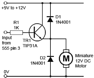
Fig. 4.6.4 Simple Motor Drive Circuit
Simple Motor Drive Circuit
Although a maximum output current from pin 3 of a standard NE555 (other versions vary) is 200mA, the maximum power dissipation of the 555 is given as 600mW. This would assume that the maximum output voltage was no more than:
600exp-3W / 200-3A = 3V
If a motor is to be driven at a higher voltage, e.g. 9V and the maximum power dissipation of the 555 is to be kept within the 600mW limit either the output current or the output voltage must be limited, for example:
600exp-3W / 9V = 67mA
So even some small DC motors may easily exceed the drive capability of the 555. In such cases a simple drive circuit such as that shown in Fig. 4.6.4 may solve the problem. It consists of a TIP31A NPN power transistor connected in emitter follower mode to the 555 output via a 1K resistor so the 555 has to supply only sufficient current to the base of the transistor to turn it fully on. The transistor will then provide sufficient current via its low impedance emitter output, to drive a motor (or other low impedance devices such as loudspeakers).
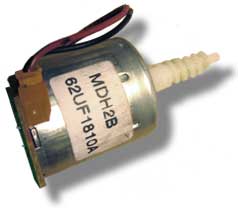
Fig. 4.6.5 Miniature DC Motor
Because the motor is an inductive load, some protection must be provided for the transistor against high voltage spikes due to back e.m.f. This is achieved by D1, which will conduct if any large positive spike, due to back e.m.f. occurs as the motor is switched off. Also D2 will prevent the emitter becoming more negative than 0V, protecting the transistor in the presence of any negative going spikes. This circuit can be added to the circuit in Fig.4.6.1, as shown in Fig. 4.6.6.
