
Google Ads
Module 6.4
Triac Circuits
- After studying this section, you should be able to:
- Describe Phase Control in triac circuits:
- Describe Hysteresis in basic triac control circuits:
- Understand how hysteresis may be minimised in triac circuits:
- Understand timer based circuits for triggering sensitive gate triacs.
Basic Diac-Triac Dimmer Circuit
A basic power control circuit using a triac and diac is shown in Fig. 6.4.1. The capacitor C1 is charged via the variable resistance comprising R1 and R2, in either a positive or negative direction alternately by the AC input voltage. Current pulses created by the diac each time the capacitor voltage (VC) reaches either the positive or negative break over potential of the diac (+/-VBO) are used to trigger a triac. The time (or phase angle) at which this happens will depend on how quickly the voltage across the charging capacitor C1 in Fig. 6.4.1 charges up. This is controlled by the variable resistor R2 and creates a variable 'Phase Control' method similar to that described in SCR Module 6.2 for SCR triggering. The AC mains waveform is effectively delayed or phase shifted by the RC circuit so that the diac is triggered by a discharge of current from the capacitor C1 into the triac gate. The triac then conducts for the remainder of the mains half cycle, and when the mains voltage passes through zero it turns off. Some time into the next (negative) half cycle, the voltage on C1 reaches break over voltage in the opposite polarity and the diac again conducts, providing an appropriate trigger pulse to turn on the triac. By varying the point in the waveform at which the triac is triggered in this way, the amount of power delivered to the load can be varied.
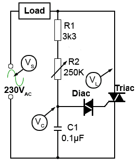
Fig.6.4.1 Basic Triac Phase
Control Circuit
Phase Shift Control
Using a basic design such as that shown in Fig 6.4.1, adjustment of the power output is possible by varying the amount of phase shift produced by the RC phase shift network R (comprising R1 and R2) and C1. As R2 is adjusted the total resistance (R) will vary between 3.3K ohms when R2 is at zero ohms, and 253.3K when R2 is at maximum resistance and producing a phase shift of almost 90°.
The value of C1 is chosen so that when it is charged up to at least the break over voltage of the diac (VBO) it can supply enough current for the diac to trigger the triac without being totally discharged. However, as the phase shift of the AC waveform across C1 increases towards 90°, the amplitude of the phase shifted wave will decrease, (as can be seen by comparing Figs. 6.4.2. and 6.4.3) but its minimum amplitude must still be equal to or greater than VBO.
The value of R1 is chosen to give only a few degrees of phase shift when R2 is adjusted to zero ohms, and the maximum value of R2 is selected so that together with R1, the amount of phase shift produced is as close to 90° as possible without letting the peak to peak voltage of the waveform VC fall below +VBO and -VBO.
Maximum Power (R2 at Minimum Resistance)
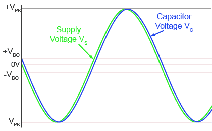
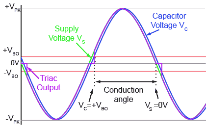
Fig.6.4.2 Waveforms at Minimum Resistance
(Mouse over or tap to reveal output waveform)
Fig.6.4.2 Waveforms at Minimum Resistance
Typical waveforms for the triac phase control circuit in Fig.6.4.1 are shown in Fig. 6.4.2 and Fig. 6.4.3. Figure 6.4.2 shows the supply voltage (VS) and the phase shifted voltage (VC) appearing across the capacitor C1 when R2 is set at minimum resistance. Note that there is very little difference between VS and VC. The blue waveform (VC) is approximately the same amplitude as VS (shown in green), and the phase shift is not much greater than 0°. Hover the PC mouse over Fig 6.4.2 (or ´touch´ on a touch screen) to view the effect on the output waveform.
The triac output waveform (purple) shows that the triac is triggered early in the positive half cycle at the point where VC = +VBO (the diac positive break over voltage,) which will be approximately +30V, depending on the diac used. At this point capacitor C will discharge current into the diac, causing a positive trigger pulse at the triac gate. The triac switches on and the output waveform is then practically identical to the supply voltage VS (apart from the very small voltage drop across the triac) until VS returns to 0V at the end of the positive half cycle when, because the current through the triac is now less than the triac´s holding current, the triac switches off.
A short time later, the triac switches on again when VC = -VBO (the diac negative break over voltage,) at about -30V, C discharges current into diac and the triac swiches on once more. The result is that the output waveform is practically the same as the input waveform apart from two short periods of time around the time the waveform passes through zero volts. This therefore applies maximum power to the load, which will be indistinguishable to applying full mains (line) potential to the load.
Minimum Power (R2 at Maximum Resistance)
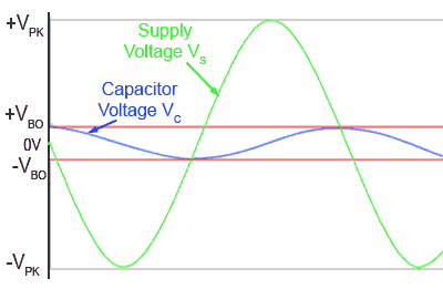
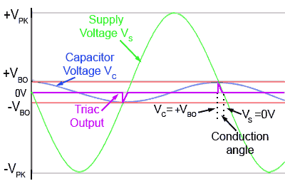
Fig.6.4.3 Waveforms at Maximum Resistance
(Mouse over or tap to reveal output waveform)
Fig.6.4.3 Waveforms at Maximum Resistance
Fig. 6.4.3 shows the phase control waveforms relating to Fig. 6.4.1 with R2 at maximum resistance (250KΩ). Here the RC network (R1+R2)C has caused a phase shift of nearly 90° but reduced the amplitude of Vc so that it is still just enough to cause the peaks of the wave to reach VBO so that the triac can still be triggered. Looking at the output wave (mouse-over or touch Fig. 6.4.3) it can be seen that when the capacitor voltage VC coincides with -VBO close to the end of a negative half cycle of VS the triac is triggered and the triac output voltage takes up the instantaneous value of VS. As VS is already close to zero volts, the triac switches off again as its current drops below the holding current (IH) to zero. The triac remains in its off condition until it is triggered once more as VC coincides with +VBO, so starting another very short, but this time positive pulse at the end of the positive half cycle. The triac output is therefore at its minimum condition.
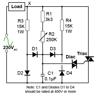
Fig 6.4.4. Eliminating Hysteresis in Triac Dimmers
Hysteresis Problems
There is however a problem with this basic triggering circuit, although it is widely used in many domestic lamp dimmers. The problem occurs because when C1 is partially discharged into the diac there will be some charge remaining on C1 and when VS passes through zero and begins to charge C1 in the opposite polarity, this remaining charge will oppose the build up of the opposite polarity charge on C1. Therefore triggering during the next half cycle will be delayed, causing unequal conduction angles, especially during the initial turn on cycles of the mains waveform. This hysteresis effect causes a difference between the amount of conduction occurring in the positive and negative half cycles, which also means that the AC wave at the triac output will not be centred on zero volts, but will effectively have a varying and unwanted DC component.
This hysteresis effect can be eliminated however, using the circuit from a detailed application note from Littelfuse shown in Fig. 6.4.4. Here the capacitor C1 is fully discharged every time VS passes through zero. If the charge on the top plate of C1 is positive and point X is at zero volts, C1 will discharge to 0V via D3 and R4. If the charge on C1 is negative when X = 0V, C1 will be discharged via D1 and R3. When point X is either positive or negative C1 cannot be charged via D1 or D3 as the voltages at the bottom of R3 and R4 will be held within about +/-0.6V of zero due to the forward conducting voltage of either D2 (during the positive half cycle) or D4 (during the negative half cycle). C1 is therefore always charged via R1 and R2.
Note that in practical control circuits using Thyristors, Triacs and Diacs, large voltages are switched very rapidly. This can give rise to serious RF interference, and steps must be taken in circuit design to minimise this. Also as mains (line) voltage is present in the circuit there must be some form of safe isolation between the low voltage control components (e.g. the Diac and phase shift circuits) and the mains ´live´ components, e.g. the triac and load. This can easily be achieved by "Opto-coupling" a low voltage control circuit to the high voltage power control part of the circuit, and/or using isolating components such specially designed pulse transformers as described in SCR Module 6.2
Triggering a Sensitive Gate Triac
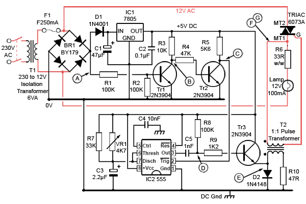
Fig. 6.4.5 Triggering a Sensitve Gate Triac
Fig. 6.4.6 Triggering a Sensitive Gate Triac
Fig. 6.4.6 Video not available in print format
The circuit in Fig. 6.4.5 demonstrates a low voltage dimmer control by triggering a SN6073A sensitive gate triac in quadrants II and III. Control is achieved over practically 180° of both positive and negative half cycles of the wave as shown in the video Fig. 6.4.6. and the circuit waveforms in Fig. 6.4.7.
Fig. 6.4.5 uses a variation on the low voltage triggering techniques demonstrated for SCR triggering in Thyristor Module 6.2 but this time driving a sensitive gate triac, which is triggered from a low voltage analogue circuit comprising a transistor zero crossing detector (Tr1), which switches off each time waveform A falls close to 0V, producing a series of positive pulses at its collector (waveform B), coinciding with the AC wave zero crossing points. These pulses are then inverted by an inverting amplifier (Tr2) to produce negative going synchronising pulses (waveform C) are used to trigger a variable delay monostable (555 timer IC1) to produce variable width square pulses having a width (and therefore time delay) controlled by VR1. The square pulses produced by IC2 are conditioned by a differentiator C5/R8 to produce narrow positive and negative going pulses (waveform D). These pulses are amplified by a current amplifier (emitter follower) Tr3 and the unwanted positive part of the waveform is removed by D2. The resulting negative going pulses drive the triac gate via an isolating pulse transformer T2 (waveform E). The whole trigger circuit is fed from a 12V AC source derived from the isolating transformer T1. The bridge rectifier BR1 supplies a 100Hz half wave waveform for the zero crossover detector, and a 5V DC stabilised supply via D1 and IC1, eliminating the need for a second low voltage DC supply. Fig 6.4.7 also shows the triac output waveforms at maximum power (F) and minimum power (G).
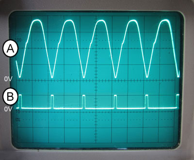
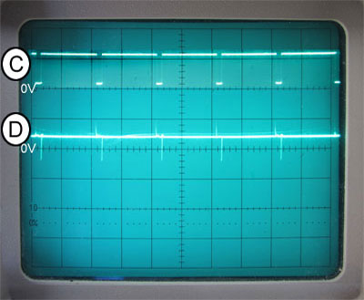
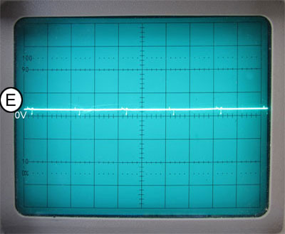
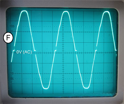
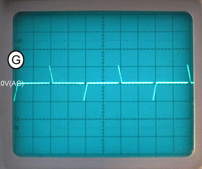
Fig. 6.4.7 Sensitive Gate Triac Triggering and Output Waveforms