
Google Ads
Module 6.6
Opto Triacs and Solid State Relays.
- After studying this section, you should be able to:
- Describe typical uses for Opto Triacs:
- • Electrical isolation.
- • Switching capability.
- • Typical construction.
- Describe typical features of Solid State Relays:
- • Electrical isolation.
- • Switching AC and DC loads.
- • Typical parameters.
- Describe typical safety features used in solid state relays (SSRs):
- • Reverse Polarity Protection.
- • Over Voltage Protection.
- • Transient Voltage Suppression.
- • Snubber circuits.
- • Zero voltage crossing.
- Describe Basic measures for testing IC based Optocoupled devices.
- • Basic tests.
- • Safety considerations for medium and high voltage devices.
Opto Triacs
Devices that are used in the control of high voltage/high power equipment need to have good electrical insulation between their high voltage output and low voltage input. Relying on a layer of silicon oxide, a few atoms thick to provide the required insulation is not really an option in such conditions. When faults occur (and they are more likely to do so in high power circuits) the results can be catastrophic, not only to the circuit components but also to the users of such equipment. Physical isolation (meaning that there is no electrical connection at all between the input and output) is what is needed. Fortunately there are readily available solutions to this problem. Many high power circuits today are controlled by low voltage, low current circuits such as microprocessors, using opto electronic devices such as Opto−Triacs, Opto−Thyristors and Solid State Relays to isolate the low and high power circuits.
The control device must be able to handle the high voltages, including very high voltage spikes that may occur in either AC or DC output circuits due to back emf from inductive loads and voltage spikes that may be randomly present on the mains (line) power supply. Also high values of surge current (much higher than the normal 'running current') that occur for example when loads such as motors or incandescent lamps are switched on, can require that the control device must be rated to handle surge currents up to 40 or 50 times higher than normal ´running´ current. The control device chosen must also ensure electrical isolation between the input and output circuits. In addition to these criteria, the circuit around the control device must also provide safeguards against dangerous situations. For example, adequate heat sinks for the solid-state devices used. Also special very fast acting fuses or circuit breakers are needed to prevent damage to the semiconductors due to current overloads.
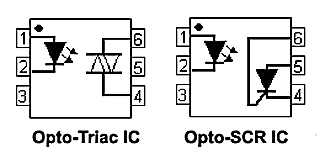
Fig. 6.6.1 Opto Triac & Opto SCR
In this group of optocouplers, photo-triacs, photo-SCRs or photo-diode/MOSFET combinations replace the photodiodes and phototransistors described in Opto Coupled Devices Module 5, and are also readily available in integrated circuit (I.C.) form for switching relatively low power AC or DC loads. High power solid state relays (SSRs) illustrated in Fig. 6.6.2 use ICs such as those shown in Fig. 6.6.1 with extra ´built in´ circuitry to handle high voltage, high current loads safely and reliably.
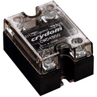
Fig. 6.6.2 Typical High Power SSR
Solid State Relays
Opto triacs and Opto SCRs are used for switching AC loads but solid state relays using power MOSFET transistors that can switch AC or DC are also available. Low power solid state relays, consisting basically of an opto triac circuit, such as the type illustrated in Fig. 6.6.1 can be used as conventional integrated circuits, mounted on a printed circuit board. Alternatively these low power optocouplers can be enclosed within an insulated case along with high power triacs or SCRs and extra safety components, such as heat sinks and pulse suppression components, in larger rack mounted Solid State Relays (SSRs) with just four or five screw type heavy duty terminals that can be treated as mains (line) power switches and can replace many types of electromechanical relays.
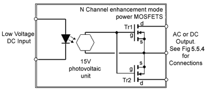
Fig. 6.6.3 MOSFET Solid State Relay
One of the most important features of SSRs is for the optocoupling to provide complete electrical isolation between its low power input circuit and its high power output circuit. When the output switch is 'open' (i.e. the MOSFETs are turned off) the SSR has a nearly infinite resistance across its output terminals, and an almost zero resistance when 'closed' (i.e. MOSFETs conducting heavily). Even so, some power will be dissipated by the semiconductor switch when in either 'on' or 'off' state with either AC or DC currents. For this reason adequate heat sinks are required to prevent overheating.
A typical circuit of a basic MOSFET SSR is shown in Figure 6.6.3. A current of about 20mA through the LED is sufficient to activate the MOSFETs that take the place of mechanical relay contacts. The (infra red) light from the LED falls on the Photovoltaic unit that comprises a number of photodiodes. Because a single photodiode will only produce a very low voltage, the diodes in the photovoltaic unit are arranged in a series/parallel array to produce sufficient voltage to turn on the MOSFETS.
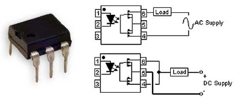
Fig. 6.6.4 Using a MOSFET Relay chip for
switching A.C. or D.C.
Figure 6.6.4 represents a basic example of a MOSFET SSR, showing how the outputs can be arranged to allow the SSR to switch either AC or DC loads. A number of similar SSRs are available to meet different AC and DC output voltage and current requirements, a typical example is the PVT412 SSR from International Rectifier (now part of Infineon Technologies) manufactured in several versions as a 6 pin DIL package and capable of replacing a single pole mechanical relay to switch AC or DC voltages up to 400V (peak) with currents up to 140mA AC or 210mA DC. Other chips are available that act as double pole, Normally Closed (NC), Normally Open (NO), and Changeover relays with a wide variety of extra facilities. SSRs are also manufactured in a range of output voltages and current ratings, with a range of package types ranging from small surface mount components through complex multi pin chips and large heavy current examples for rack mounting in electrical control cabinets. More information on SSRs can be found by searching for Solid State Relays on manufacturers websites such as Infineon Technologies or at semiconductor suppliers such as RS Components
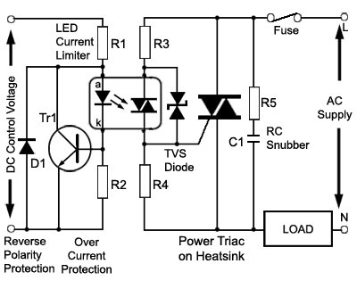
Fig. 6.6.5 Solid State Relay Safety Features
SSR Safety Features
SSRs consist basically of an optocoupler driving some high power switching device such as a power triac, MOSFETS or a SCR, but as their purpose is to switch high power electrical loads, often in safety critical situations SSRs are manufactured with a wide variety of features, designed to allow for safe and reliable operation. Some of these are illustrated in the circuit shown in Fig 6.6.5:
Reverse Polarity Protection. If the input terminals are connected in the wrong polarity, diode D1 conducts and reduces the voltage at the bottom of R1 to about 0.7V, thereby saving the optocoupler LED from damage. Note that the diode and the current limiting resistor R1 power ratings must be able to withstand the reverse polarity current at maximum input voltage without damage, otherwise a suitably rated input fuse may be inserted between the input positive terminal and the current limiting resistor.
Over Current Protection. It is common for SSRs to be able to work from a range of DC input voltages, for example 5v to 24V. These higher voltages can cause the current through the optocoupler LED to rise higher than its required maximum, in this case the over current protection circuit operates to maintain a suitable current level through the LED. R2 is a low value resistor for current sensing; it's value is chosen so that under normal operating conditions Tr1 is biased just below its cut-off threshold, but if the current through the optocoupler input LED increases due to an excessive input voltage, the extra current through R2 will cause Tr1 to conduct, diverting some of the LED current through Tr1 reducing the voltage at the bottom of R1 and the current though the LED to a safe level.
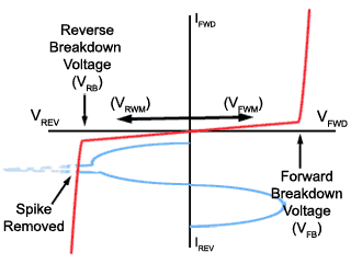
Fig. 6.6.6 Transient Voltage Suppression
Transient Voltage Suppression (TVS) Diode. SSRs used in control situations can be liable to damage caused by sudden and short lived (i.e. transient) voltage spikes, which can be caused by external events such as back emf pulses when switching inductive loads; also remote lightning discharges and other electromagnetic or electrostatic discharges are high risk occurrences for semiconductor devices. Such voltage spikes may be very short in duration but can be hundreds or thousands of volts in amplitude, and although the current they create may be very small, the stress caused by such voltages can cause total failure in the semiconductor devices used in SSRs. One way to reduce these dangerous events is the use of a transient voltage suppressor (TVS) diode connected in parallel with sensitive devices such as the optocoupler as shown in Fig. 6.6.5.
Fig. 6.6.6 illustrates the action of the TVS diode, and shows a sine wave output superimposed on the TVS diode characteristics. The bi-directional TVS diode works rather like two back to back Zener diodes, where above a certain reverse voltage, current breakdown occurs and the diode conducts heavily. As the TVS diode in this case is bi-directional, breakdown occurs in both forward and reverse conditions.
In use, a TVS diode must have a breakdown voltage higher than the peak voltage of the AC wave, which is 1.414 x VRMS so a TVS diode with a breakdown voltage about 1.5 times greater than the RMS voltage of the sine wave is normally used. A voltage spike exceeding this limit causes the diode to conduct heavily, limiting its voltage to the breakdown voltage of the diode. A notable difference between a Zener and a TVS diode is that the TVS diode has a more rugged junction area, to cope with the sudden heavy current rush during spike events. Once the spike is over however, the diode stops conducting (apart from a small reverse leakage current) and has no further effect on the output wave until any further spikes occur. TVS diodes are also available in single directional types that may also be used in the input side of the optocoupler in SSRs using a DC input if there is high risk of spikes occurring. However, because the DC input is usually fed from a smoothed DC power supply, this would normally be expected to minimise the risk, therefore the use of TVS diodes across the input components is rarely considered necessary.
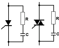
Fig. 6.6.7 RC Snubber Circuits
RC Snubber Circuits. These circuits provide a method of reducing the damaging effect of spikes occurring on the AC mains supply, or the very large and fast voltage changes that can occur when an inductive load is switched on or off (Commutated). With older types of triacs or SCRs this RC network (R5 and C1) is connected across the output triac or SCR as shown in Fig. 6.6.5 and Fig 6.6.7. Its effect is to slow the rapid increase or decrease of voltage during the spike. The use of a snubber circuit can also reduce the radio interference caused by the triac or SCR switching. By choosing a suitable time constant for R5/C1 the capacitor will not have time to charge as the spike voltage rises, before the voltage is reducing once more and discharging the capacitor. In this way the amplitude of any fast voltage spikes is reduced. Typical values for R would be about 39 to 100Ω for R5 and 22 to 47nF for C1. The capacitor would also need to be a pulse type having a very high maximum working voltage, much higher than the peak value of the output wave, to allow for the added stress caused by any voltage spikes. The design of snubber circuits is more complex however, than simply choosing typical R and C values, and must take into account a number of factors that will be unique to the circuit or component the snubber is protecting and to the loads the circuit may be driving.
A useful application note on snubber design and component calculator is provided on line by HIQUEL (High Quality Electronics).
Alternistors
Alternatively there are modern Triacs available, which can also be called ´Alternistors´ or ´Alternistor Triacs´ that are much less prone to damage or random false triggering caused by fast transient voltages. Several semiconductor manufacturers have their own range of devices, such as the ´SnubberlessTM´ range from ST Microelectronics or the ´Hi-ComTM´ range from WeEn Semiconductors that are able to handle the voltage spikes as well as the fast dV/dt events encountered during commutation (switch off) with inductive loads. The internal design of these triacs is different to the original types, making them much better at handling the fast high voltage changes that can happen as inductive loads are switched off, due to the phase difference between current and voltage in inductors. In this case it is possible that when the triac switches off as the mains (line) current passes through zero volts, the mains voltage across the triac can be at its maximum value. While such events in original triac designs could cause problems with uncontrolled re-triggering, this has been greatly reduced in modern designs.
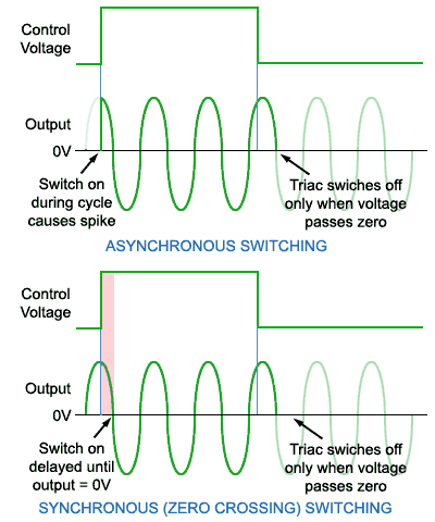
Fig. 6.6.8 SSR Zero Crossing Action
Zero Voltage Crossing. Some SSRs include 'Zero Crossing' or 'Synchronous Switching' circuits, which reduce the possibility of introducing fast changing 'spikes' onto the mains (line) supply by ensuring that their output will only switch on as the mains voltage cycle passes through zero volts. As shown in Fig. 6.6.8 if the control voltage requests a switch on at a time during the voltage cycle when the AC voltage is not passing through 0V, the switching action is delayed until the voltage next crosses 0V at end of the present half cycle. The zero voltage crossing circuit does not play any part in switching the output off however; this is controlled by the action of the triac or SCR, which once turned on will only turn off when the output load current falls below the triac or SCR's specified holding current, which it will do as the current waveform passes through zero.
The above descriptions of safety features are intended to introduce users of SSRs to some of the necessary safety constraints when choosing the right SSR for any particular operation. However this list is not offered as a comprehensive guide, the importance or non-importance of any of these factors will depend very much on the intended use of the SSR. It is advisable therefore, especially when considering the safe operation of circuits, to obtain advice specific to the intended project, many manufacturers or national and international safety agencies can readily give qualified advice on the suitability of SSRs for particular uses. You are also encouraged to further study by following some of the recommended links at the bottom of this page.
Solid State and Mechanical Switching Compared
Solid State Relays (SSRs) have a number of advantages over electromechanical relays, some of which are obvious advantages and some that would be disputed by adherents to (and manufacturers of) electromechanical relays. Which type of relay is better for a particular application however, depends more on the application rather than the type of relay. This should therefore be carefully considered when reading the following lists.
Advantages of SSRs against electromechanical relays.
- Because SSRs have no inductive coils or moving contacts they do not generate electromagnetic interference.
- SSRs do not cause any potentially dangerous arcing.
- SSRs are silent in operation.
- SSRs are not subject to mechanical wear, so will potentially perform many more switching operations than electromechanical relays (however either type may be designed to perform more operations than is required during the lifetime of the equipment they are used in).
- SSRs do not suffer from contact bounce.
- SSRs have a faster switching time than electromechanical relays.
- For switching AC, Zero Crossing SSRs are available that only switch on at, or close to the time when the AC waveform passes through zero volts, so reducing the occurrence of voltage spikes that occur if a circuit is switched on when the AC voltage is at a maximum.
- SSRs can be physically smaller than comparable types of electromechanical relays.
Disadvantages of SSRs against electromechanical relays.
- When SSRs are switched on there is a measurable resistance between the output terminals, therefore SSRs produce some heat as well as a voltage drop in their ‘on’ condition.
- When SSRs are in their ‘off’ state, there is still a small reverse leakage current flowing in the output. Unlike electromechanical relays, SSRs are therefore neither totally ‘on’ or ‘off’. Therefore they may not be permitted for use under some safety regulations.
- Because SSRs are able to switch on very quickly (in milliseconds) random interference spikes in their input circuits or sudden fast voltage changes at their outputs can cause unwanted switching of some SCRs or triacs.
- Failure of an SSR will usually cause a short circuit (switch on) whereas failure in an electromechanical relay will usually cause an open circuit (switch off). Because of this, using SSRs may cause some concern in safety critical systems.
Further information
Solid State Relays vs Electromechanical Relays - Application Notes Solid State Patronise USA
How to choose the right relay - National Instruments
Tech tips on relays-Crydom Inc.