Module 2.1
Shunt Voltage Regulators
- After studying this section, you should be able to:
- Understand the principles of shunt regulators.
- • Regulating action of a zener diode.
- • Operation of the basic shunt regulator circuit.
- • Calculate component values for a basic shunt regulator circuit.
- Recognise the limitations of the basic shunt regulator.
- Understand methods for increasing current rating.
- Recognise cascading techniques for improving line regulation.
Basic Shunt Regulator Circuits
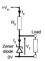
Fig. 2.1.1 Basic Shunt
Regulator
Shunt regulators are widely used because they are cheap, effective and simple. It is unusual however, to find a shunt regulator used as the main regulating circuit in a large power supply. Shunt regulation is only really suitable, at reasonable cost, for relatively small currents and a range of fixed, usually fairly low voltages. This is due to a disadvantage of shunt regulation, which is that a regulation current (flowing through the zener diode) must always be flowing in addition to the load current. This is wasteful of power if large currents are involved.
The basic shunt regulator circuit is shown in Fig. 2.1.1 and consists of only two components; a series resistor RS feeding current to a zener diode, which is connected in reverse polarity) across the load.
The Zener Diode.
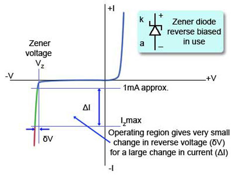
Fig. 2.1.2 Zener Diode Characteristic Curve
The main property of a zener diode is that the voltage across the diode (VZ) will remain practically steady for a wide range of current (IZ) when the diode is operated in reverse bias mode, as shown in Fig. 2.0.1.
Fig. 2.1.2 illustrates the characteristic curve of a zener diode where the operating region (shown in green) of the zener diode is a range of current on the nearly vertical breakdown region of the curve.
Provided that the reverse current is kept at a value above about 1 to 2mA (avoiding the "knee" of the reverse characteristic) and does not exceed the safe working current for that particular diode type, very little change in reverse voltage takes place. It is this effect that is used to give the required regulating effect.
As the power supply operates, two conditions may occur to change the output voltage;
a. The load current may vary.
b. The supply voltage may vary.
The circuit is arranged so that the total supply current IS is made up of the output load current IOUT plus the current in the zener diode IZ:
IS = IZ + IOUT
Provided that the zener diode is working within its allowable range of current, the voltage VZ will remain practically constant, deviating by only a very small amount (δV).
Point of Load Regulators
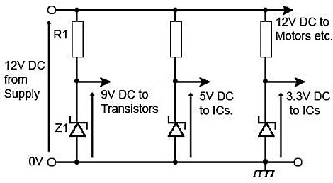
Fig. 2.1.3 Point of Load Regulators
The most common method of using these basic zener diode shunt regulators is the ‘point of load’ regulation system. This method uses a number of fixed voltage, relatively low current regulators at various points around the circuit being supplied. A relatively ineffective main regulator can then be used in the power supply unit because each section of the circuit has its own regulator. For example many complex circuits need different voltage levels for different electrical and electromechanical parts. Each may have its own regulated supply, e.g. 9V, 5V or 3.3V, using "point of load" shunt regulators fed from a single common supply, as shown in Fig. 2.1.3. Each of the voltage regulators will normally be placed as close to the circuit supplied as physically possible, and have additional decoupling capacitors to reduce any noise or cross talk between the individual supply lines.
Variations in Load Current
If the current in the load Iout tends to fall, the voltage across the load would tend to rise, but because it is connected in parallel with the diode the voltage will remain constant. What will change is the current (IZ) through the diode. This will rise by an amount equal to the fall of current in the load. The total supply current IS being always equal to IZ + IOUT. An increase in load current IOUT will likewise cause a fall in zener current IZ, again keeping VZ and the output voltage steady.
Variations in Input Voltage
If the input voltage rises this will cause more supply current IS to flow into the circuit. Without the zener shunt regulator, this would have the effect of making the output voltage Vout rise, but any tendency for VOUT to rise will simply cause the diode to conduct more heavily, absorbing the extra supply current without any increase in VZ thus keeping the output voltage constant. A fall in the input voltage would likewise cause a reduction in zener current, again keeping VOUT steady.
Limitations
This simple shunt regulator is only suitable for relatively small currents and a fixed range of voltages. There are a number of limitations to the use of this circuit:
Output voltage:
The output voltage is equal to the zener voltage of the diode and so is fixed at one of the available voltage levels.
Output current:
If the output current falls to zero for any reason (the load may become open circuit due to a fault, or be disconnected from the power supply), all of the load current must be passed by the zener diode. Therefore the maximum current available for the load must be no greater than the maximum safe current for the zener diode alone.
Input voltage:
The input voltage must be higher (usually about 30% higher) than the output voltage to allow regulation to take place. It should not be too high however, as this will result in more power being dissipated by the diode.
Power dissipation:
The power dissipated in the diode must be kept within the safe working limits for the device chosen. Maximum power will be dissipated if the load is allowed to go open circuit while the input voltage is at its maximum value. This ‘worst case’ should not exceed the diode‘s maximum power rating.
The above limitations are controlled by the suitable choice of zener diode and series resistor RS. The design of simple regulator circuits is fairly straightforward if a few simple steps are followed:
1. Decide on a zener diode of the required voltage.
2. Select a diode whose maximum current at least matches, and preferably exceeds the maximum current requirement of the load.
Note: Zener diode ratings usually quote maximum power dissipation rather than current, so you will need to work out the current rating from the power and voltage given for the device.
3. Find out the highest voltage likely to occur at the supply input. (VIN max)
4. Calculate the value of a suitable series resistor RS by using the formula:

Where:
VIN max = the highest likely input voltage.
VZ = the zener diode voltage
IOUTmax = the maximum output current.
IZ min = the minimum current at which the zener will operate (say about 1 to 2mA).
5. Calculate the power dissipated in the series resistor (RS) by the formula:
Power dissipated by RS = VR x IIN
Note: When calculating power ratings and resistances, your answers will probably not exactly match the commercially available preferred values. Therefore choose the closest preferred value, and then put this value into your calculations to make sure the circuit will operate correctly with the preferred value. You should then be able to quote:
A suitable resistor value and its power rating and a suitable zener diode type number.
Example:
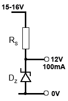
Fig. 2.1.4 Example
Design a simple zener diode (see Fig. 2.1.4) shunt regulator circuit with the following specifications:
Maximum load current required. 100mA
Output voltage. 12V
Input voltage. 15V nominal, 16V max.
Assuming a minimum zener current of 1mA
The problem can be solved in 4 steps.
1. Find a value for RS
RS must supply sufficient current to keep IZ at or slightly above 1mA when the zener diode is passing its minimum current.
As the total circuit current IIN = IOUT + IZ
The minimum zener diode current will occur when the input voltage (VIN) is at its minimum value and the load current (IOUT) is at its maximum value.
Under these conditions the current (IIN) flowing through RS will be IOUT max + IZ min
Which is 100mA + 1mA = 101mA
As R = V/I and the voltage across RS = VIN min - VZ
Then RS = (VIN min - VZ)/IIN = (15 -12) / 101exp-3 = 29.7Ω
Therefore a practical value for RS will be the next lowest preferred value 27Ω)
2. Calculate the maximum current (IIN max) that will pass through RS.
The maximum current (IIN max) will occur when VIN is at nits maximum value, i.e. 16V
IIN max = (VIN max - VZ) / RS = (16 - 12) / 27 = 4 / 27 = 148mA
3. Calculate the maximum power requirement for RS
This will occur when VIN is at its maximum value).
(VIN max - VZ) x IIN max = (16 - 12) x 148exp-3 = 0.592W
A practical power rating for RS will therefore be the next highest available power rating = 1W)
4. Calculate the maximum power (PZ max) that must be dissipated by the zener diode.
This will be the power that the zener diode would need to dissipate if the load was disconnected while the input voltage was at maximum, causing the maximum current (IIN max) of 148mA to flow through the vener diode.
As Power P = I x V, then PZ max = IIN max x VZ = 148exp-3 x 12 = 1.776 = approx. 1.8W
A suitable shunt regulator would therefore consist of a 27Ω 1W resistor and a 12V zener diode with a power rating of at least 2Watts.
However, it is interesting to compare the power delivered to the load, (12V x 100mA) = 1.2W with the power dissipated in shunt regulator, (0.592W in the resistor + 1.776W in the diode = 2.368W.
Only about 33% of the total power is in the load with about 66% being dissipated by the shunt regulator!
The simple zener diode shunt regulator is therefore not very efficient when handling even these amounts of current. A better option can be to add a transitor to the circuit to handle larger currents.
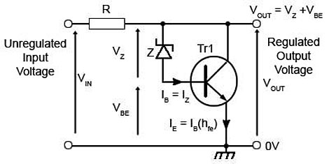
Fig. 2.1.5 Transistor Shunt Regulator
Large Current Shunt Regulators
The current that can be handled by the simple zener diode/resistor shunt regulator is limited by the maximum current rating of the zener diode, but there are ways of increasing the maximum current capability of shunt regulators. One typical method is given in Fig. 2.1.5 where a power transistor, capable of passing an emitter current much larger than the zener diode is used.
The zener diode now only handles the transistor base current and the main stabilising current IE is approximately equal to the base current of the transistor, multiplied by the hfe of the transistor:
IE = IB(1+hfe)
Therefore the regulator can handle IZ (1+hfe) amperes, allowing much larger load currents to be supplied by the regulator.
Note that the output voltage is no longer equal to VZ but to VZ+VBE. The transistor will have a VBE of typically 0.7V, so to produce a 5V regulator, a zener diode of 4.3v would be chosen.
Operation
If the current in a load attached to the regulator output decreases, the voltage at the right hand end of the series resistor (R) will tend to increase. When this happens, the base-emitter voltage of the transistor will increase by a similar amount, as the voltage across the zener diode is constant.
This increase in base-emitter voltage will cause the transistor (Tr1) to conduct more heavily until the extra current taken by the transistor balances the reduction in current taken by the load, the output voltage of the regulator is therefore returned to its previous ‘normal’ value.
If the load current increases, a similar action takes place, but this time there will be a reduction in Tr1 base voltage. This will reduce current through the transistor, thereby balancing the increase in load current. Again, the output voltage of the regulator remains relatively constant.
Improving Line Regulation
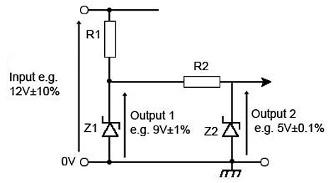
Fig. 2.1.6 Cascaded Shunt Regulators
An effective regulator circuit should compensate for variations in input voltage as well as variations in output voltage (Output stabilisation). These input variations may be due to changes in the AC mains (line) supply, hence the name line regulation, or changes in the rectified DC input to the regulator circuit caused by variations in current drawn by other parts of the electronic system sharing the same supply. How well line regulation works can be determined by comparing any change in the regulator output voltage with the change in regulator input voltage (assuming a constant load current). This can be expressed as the line regulation factor, and quoted as a percentage. For example if the input voltage to the regulator changes by ±2V but the output voltage only changes by ±0.2V the line regulation factor is ±10%.
Fig. 2.1.6, shows how line regulation can be improved by using a series of zener diode regulators connected in cascade, each one will have a lower voltage that the previous one, but by connecting regulators in cascade, the overall regulation factor is the product of the factors of the individual circuits. Therefore two regulators each having a regulation factor of 10% or 0.1 would give an overall factor of 0.1 x 0.1 = 0.01 or 1%.


