
Module 3.3
How a BJT (Bipolar Junction Transistor) Works
- After studying this section, you should be able to:
- • Describe the basic operation of a silicon planar transistor.
- • Understand the operation of the base/emitter and base/collector junctions.
- • Describe the effects of doping in the transistor materials.
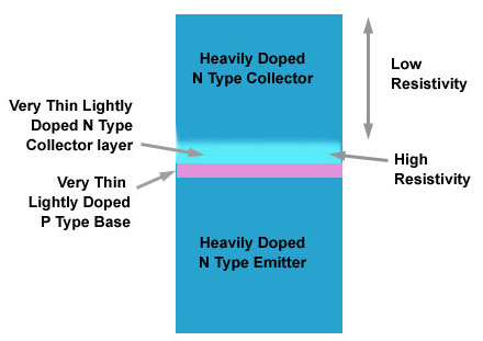
Fig 3.3.1 How a BJP Transistor is Doped.
Its all in the doping

The way a transistor works can be described with reference to Fig. 3.3.1 which shows the basic doping of a junction transistor and Fig. 3.3.2 showing how the BJT works.
The operation of the transistor is very dependent on the degree of doping of the various parts of the semiconductor crystal. The N type emitter is very heavily doped to provide many free electrons as majority charge carriers. The lightly doped P type base region is extremely thin, and the N type collector is very heavily doped to give it a low resistivity apart from a layer of less heavily doped material near to the base region. This change in the resistivity of the collector, ensures that a large potential is present within the collector material close to the base. The importance of this will become apparent from the following description.
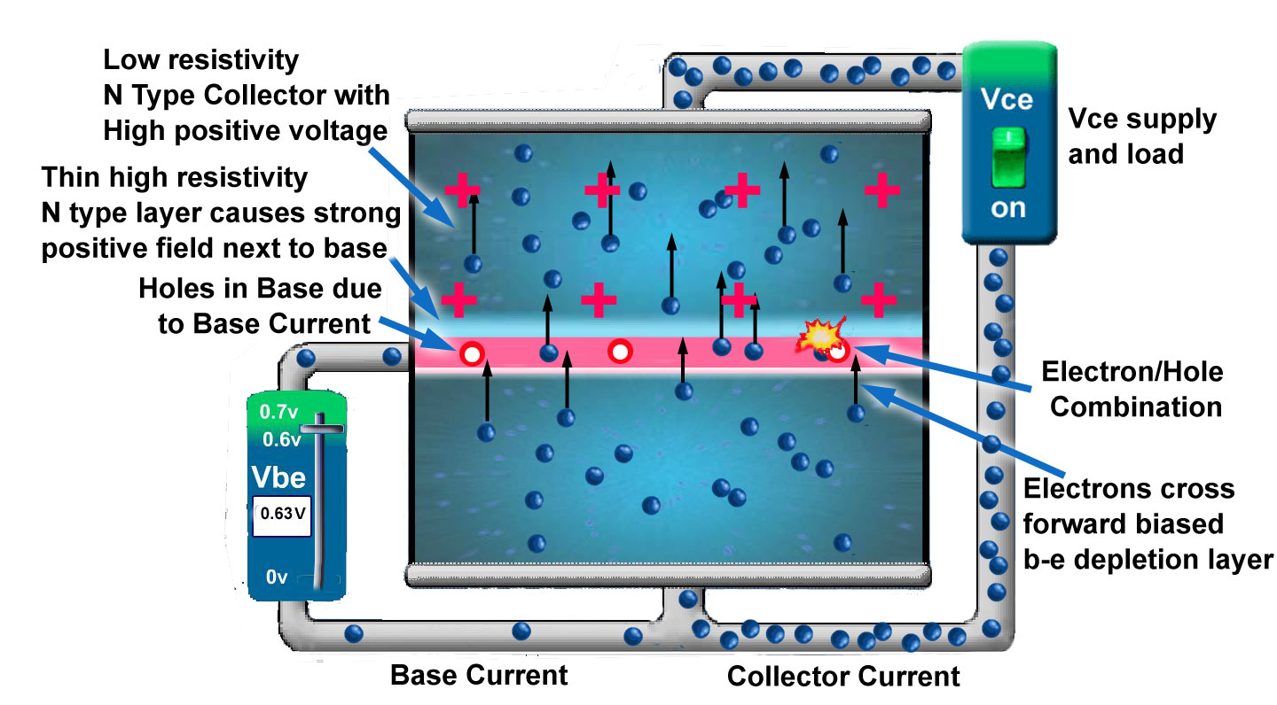
Fig 3.3.2 How a Transistor Amplifies Current.
During normal operation, a potential is applied across the base/emitter junction so that the base is approximately 0.6v more positive than the emitter, this makes the base/emitter junction forward biased.
A much higher potential is applied across the base/collector junction with a relatively high positive voltage applied to the collector, so that the base/collector junction is heavily reverse biased. This makes the depletion layer between base and collector quite wide once power is applied.
As mentioned above, the collector is made up of mainly heavily doped, low resistivity material with a thin layer of lightly doped, high resistivity material next to the base/collector junction. This means that most of the voltage between collector and base is developed across this thin high resistivity layer, creating a high voltage gradient near the collector base junction.
When the base emitter junction is forward biased, a small current will flow into the base. Therefore holes are injected into the P type material. These holes attract electrons across the forward biased base/emitter junction to combine with the holes. However, because the emitter region is very heavily doped, many more electrons cross into the P type base region than are able to combine with the available holes. This means there is a large concentration of electrons in the base region and most of these electrons are swept straight through the very thin base, and into the base/collector depletion layer. Once here, they come under the influence of the strong electric field across the base/collector junction. This field is so strong due to the large potential gradient in the collector material mentioned earlier, that the electrons are swept across the depletion layer and into the collector material, and so towards the collector terminal.
Varying the current flowing into the base, affects the number of electrons attracted from the emitter. In this way very small changes in base current cause very large changes in the current flowing from emitter to collector, so current amplification is taking place.
Watch our Video on how bipolar transistors are made and How they Work.