Google Ads
Module 5.0
Opto Coupled Devices
- After studying this section, you should be able to:
- Describe the operation of a photo transistor
- Describe typical uses for photo couplers.
- Describe the advantages and disadvantages of different optocouplers:
- • Photo transistor types.
- • Photo diode types.
Opto Devices & Photo transistors
Fig. 5.0.1 Transistor Optocouplers
& Opto Sensors
Optocouplers or opto isolators consisting of a combination of an infrared LED (also IRED or ILED) and an infra red sensitive device such as a photo diode or a photo transistor are widely used to pass information between two parts of a circuit that operate at very different voltage levels. Their main purpose is to provide electrical isolation between two parts of a circuit, increasing safety for users by reducing the risk of electric shocks, and preventing damage to equipment by potential short circuits between high-energy output and low-energy input circuits.
They are also used in a number of sensor applications to sense the presence of physical objects.
Transistor Optocouplers
The devices shown in Fig. 5.0.1 use photo transistors as their sensing elements as they are many times more sensitive than photo diodes and can therefore produce higher values of current at their outputs.
Example 1 in Fig. 5.0.1 illustrates the simplest form of opto coupling consisting of an infrared LED (with a clear plastic case) and an infrared photo transistor with a black plastic case that shields the photo transistor from light in the visible spectrum whilst allowing infrared light to pass through. Notice that the photo transistor has only two connections, collector and emitter, the input to the base being infrared light.
Examples 2 and 3 in Fig 5.0.1 are typical opto coupled devices widely used as position and proximity sensors, these are used as optically activated switches and are described in more detail in Module 5.4.

Fig. 5.0.2 The 4N25 Optocoupler
Example 4 in Fig. 5.0.1 is a 4N25 opto coupler in a 6 pin DIL integrated circuit from Vishay. It uses an output photo transistor with a base connection that is also connected to an external pin for applying an external circuit if required. This allows the opto coupler to have a DC bias applied to prevent the transistor from producing current at very low light levels. Biasing the photo transistor can also enable it to be used with signals such as analogue audio, as described in Module 5.3. In this case the emitter connection can be left unconnected and the base connection used as an output, then the output photo transistor collector/base junction operates as a photo diode, greatly increasing the frequency range of the opto coupler, but at the expense of greatly reducing the available signal amplitude at the output. The 4N25 can also operate as a digital opto coupler with logic 1 and logic 0 inputs. The isolation between input and output on the 4N25 is a minimum of 5.3 kV.
Example 5 in Fig. 5.0.1 is a PC817 4 pin single channel opto isolator chip from Sharp, which uses an integral infra red LED and a photo transistor to produce an output of up 50mA and provides electrical isolation up to 5kV. It is also available in 2, 3 and 4 channel versions.

Fig. 5.0.3 Basic Photo transistor Structure
Photo transistors
Fig. 5.0.3 shows the basic structure of a photo transistor Its operation is similar to the photo diodes described in Diodes Module 2.7. However because the conversion from light to current takes place in a transistor, the tiny current produced by a particular level of photon input to the base can be amplified to produce a collector current 200 times greater or more, depending on the hfe of the transistor, making the photo transistor much more efficient than a photo diode However, because of the large junction area (and therefore much higher junction capacitance) of a photo transistor, its response at high frequencies is poor, and the switching time is much slower, compared to a photo diode Also the relationship between changes in light input and changes in output voltage is not as linear as in photo diodes Consequently photo transistors, though less useful than photo diodes for high frequency data transmission, are widely used in control applications such as opto couplers/isolators, and position sensors.
Photo transistor Operation
In a photo transistor, light, in the form of photons is collected in the base layer, which occupies the major part of the visible window on the top surface of the device, as illustrated in Fig. 5.0.3. The emitter area is therefore reduced in size to maximise light absorption in the base.
The conversion between photons and current takes place largely in the depletion region around the base/collector PN junction where photons absorbed via the anti-reflective layer into the base layer dislodge electrons to create electron/hole pairs in a similar manner to that in photo diodes, but now the free electrons created by this process are the source of base current in the transistor, and are now amplified by an amount equal to the hfe of the transistor.
The N type collector immediately beneath the depletion layer has a higher resistance than the N+ layer next to the collector terminal. Because of this higher resistance close to the PN junction, there is a large voltage gradient in the collector close to the base/collector junction. This provides a higher positive voltage close to the depletion layer to attract and accelerate the negatively charged electrons in the depletion layer towards the collector terminal.
Compared to photo diodes however, photo transistors do have some drawbacks; their response to varying levels of light is not quite so linear, making photo transistors less suitable than photo diodes for accurate light measurement.
Although photo transistors can be used to detect light sources across the visible light spectrum, they are most sensitive to wavelengths in the near infrared range around 800 to 900nm, and are most often used with infrared emitting sources such as infrared emitting LEDs (also called IREDs or ILEDs) as their light source.
Photo transistors are generally not as fast as photo diodes at reacting to abrupt changes in light levels. For example, the time taken for the photo transistor output to change between 10% and 90% in response to a sudden change in light level at the input can be between 30 and 250µs whereas high speed photo diodes can have rise and fall times as low as 20ps (pico seconds) or less. Manufacturers normally quote these figures for rise time (tr) and fall time (tf) under particular conditions of temperature and collector current.
The main reason for the much slower response in photo transistors is due to the much larger area of the base/collector junction, and the fact that the capacitance that exists across this junction is further magnified by the 'Miller Effect', which causes the junction capacitance to be magnified by the current gain (hfe) of the transistor. In practice this means that the more sensitive the transistor (i.e. the larger the base area) and/or the higher the current gain of the transistor, the longer the rise and fall times will be. For these reasons photo transistors are mostly used for switching DC or low frequency AC applications.
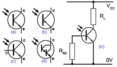
Fig. 5.0.4 Photo transistor Connections
Photo transistor Connections
Photo transistors are available in several forms such as NPN (Fig. 5.0.4a) or PNP (Fig. 5.0.4b). Many photo transistors only have connections for the emitter and collector, as the base input is provided by light; however a base connection is provided on some types (Fig. 5.0.4c).
Darlington photo transistors (Fig. 5.0.4d) are also available; using a Darlington pair transistor configuration gives even greater current gain.
At low or even no light levels, photo transistors can still produce a small amount of current due to random collisions in the depletion layer. Applying base bias as shown in Fig. 5.0.4e can have the effect of preventing this 'Dark Current', so reducing the effect of random noise and giving a better defined on/off level to the output current.
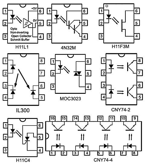
Optocouplers have many uses and are available in many varied types, a few examples are illustrated in Fig. 5.0.5. Use the type numbers to search for data sheets and use them to identify the purpose of each design.