Module 2.4
Karnaugh Maps
- After studying this section, you should be able to:
- Understand the use of Karnaugh maps.
- • Draw maps for Multi input circuits.
- • Use Gray code notation.
- • Derive Karnaugh maps from truth tables.
- Use Karnaugh Maps
- • Group Karnaugh map cells.
- • Simplify logic circuits.
- • Produce minimised Boolean equations.
- Make choices in cell selection to achieve a desired circuit result.
- • Cost reduction.
- • Propagation delay.
- Use manual and software methods for circuit minimisation.
- • Minimise complex Boolean equations using appropriate software.
Why Karnaugh Maps?
Karnaugh Maps offer a graphical method of reducing a digital circuit to its minimum number of gates. The map is a simple table containing 1s and 0s that can express a truth table or complex Boolean expression describing the operation of a digital circuit. The map is then used to work out the minimum number of gates needed, by graphical means rather than by algebra. Karnaugh maps can be used on small circuits having two or three inputs as an alternative to Boolean algebra, and on more complex circuits having up to 6 inputs, it can provide quicker and simpler minimisation than Boolean algebra.
Constructing Karnaugh Maps
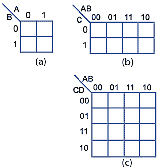
Fig.2.4.1 Karnaugh Maps
The shape and size of the map is dependent on the number of binary inputs in the circuit to be analysed. The map needs one cell for each possible binary word applied to the inputs.
Therefore:
2 input circuits with inputs A and B require maps with 22 = 4 cells (Fig 2.4.1a).
3 input circuits with inputs A B and C require maps with 23 = 8 cells (Fig 2.4.1b).
4 input circuits with inputs A B C and D require maps with 24 = 16 cells (Fig 2.4.1c).
*Important:
Notice that this edge numbering does not follow the normal binary counting sequence, but uses a Gray Code sequence where only one bit changes from one cell to the next. This is an important feature of Karnaugh maps; get the sequence wrong and the map will not work!
The input labels are written at the top left hand corner, divided by a diagonal line. The top and left edges of the map then represent all the possible input combinations for the inputs allocated to that edge.
For example, in the 3 input map (b) in Fig. 2.4.1, the top edge of the map represents the 4 possible combinations for inputs A and B, so the cells are labelled 00,01, 11, and 10 (See *Important note).
Because example (b) in Fig. 2.4.1 is a 3 input map, input C on the left hand edge only has two possible combinations, 00 and 01. This map is therefore rectangular rather than square to cover the 8 possible combinations available from 3 inputs.
Using the Karnaugh Map
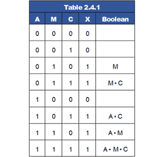
The Karnaugh map can be populated with data from either a truth table or a Boolean equation.
As an example, Table 2.4.1 shows the truth table for the 3 input ‘cash room’ example, together with the Boolean expressions derived from each input combination that results in a logic 1 output. This results in a Boolean equation for the un-simplified circuit:
X = M + M•C + A•C + A•M + A•C•M
This table will serve to show the process of transferring the data from Table 2.4.1 into the cells of the Karnaugh map. The process is shown step by step in Fig. 2.4.2
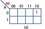
Step (a)
From Table 2.4.1 row 3, inputs AMC have values of 010, producing a logic 1 at the output (X) and giving the Boolean expression M in the Boolean column. Therefore 1 is placed in the map cell corresponding to A=0 and MC=10 as shown at (a) in Fig. 2.4.2.
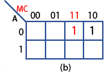
Step (b)
In Table 2.4.1 row 4, inputs AMC have values of 011, producing a logic 1 at the output (X) and giving the Boolean expression MC in the Boolean column. Therefore 1 is placed in the map cell corresponding to A=0 and MC=11 as shown at (b) in Fig. 2.4.2.
Step (c)
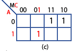
In Table 2.4.1 row 5, output (X), is 0 so this row is ignored. However, in row 6, inputs AMC have values 101, producing a logic 1 at the output (X) and giving the Boolean expression AC in the Boolean column. Therefore 1 is placed in the map cell corresponding to A=1 and MC=01 as shown at (c) in Fig. 2.4.2.
Step (d)
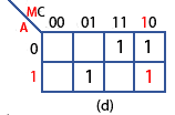
In Table 2.4.1 row 7, the inputs AMC have values of 110, producing a logic 1 at the output (X) and giving the Boolean expression AM in the Boolean column. Therefore 1 is placed in the map cell corresponding to A=1 and MC=10 as shown at (d) in Fig. 2.4.2.
Step (e)
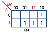
Finally, in Table 2.4.1 row 8 the inputs AMC have values of 111 producing a logic 1 at the output (X) and giving the Boolean expression of AMC in the Boolean column. Therefore 1 is placed in the map cell corresponding to A=1 and MC=11 as shown at (e) in Fig. 2.4.2.
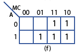
Fig.2.4.2 (a)−(f) Populating the Karnaugh map
The completed map (f)
All the truth table rows that produced a logic 1 have now been entered into the map and those lines that produced a logic 0 can be ignored, so the remaining three cells are left blank. Later it will be shown that these blank cells can be useful when mapping larger circuits, but for now the map is ready for simplification.
Simplifying Karnaugh Maps
Circuit simplification in any Karnaugh map is achieved by combining the cells containing 1 to make groups of cells. In grouping the cells it is necessary to follow six rules.
How these rules are applied is illustrated using a four input 16-cell map shown in Fig. 2.4.3.
Karnaugh Map Rules
1. Groups should contain as many ‘1’ cells (i.e. cells containing a logic 1) as possible and no blank cells.
2. Groups can only contain 1, 2, 4, 8, 16 or 32... etc. cells (powers of 2).
3. A ‘1’ cell can only be grouped with adjacent ‘1’ cells that are immediately above, below, left or right of that cell; no diagonal grouping.
4. Groups of ‘1’ cells can overlap. This helps make smaller groups as large as possible, which is an advantage in finding the simplest solution.
5. The top/bottom and left/right edges of the map are considered to be continuous, as shown in Fig. 2.4.3, so larger groups can be made by grouping cells across the top and bottom or left and right edges of the map.
6. There should be as few groups as possible.
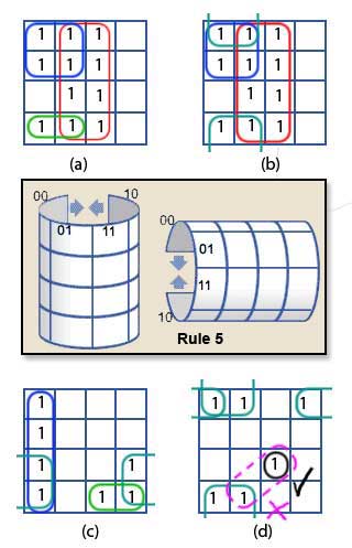
Fig.2.4.3 Typical Karnaugh Groups
Map (a) follows rules 2, 3 and 4 and shows three groups containing 8, 4 and 2 cells. This will simplify the circuit being produced, but it is not optimum.
Map (b) shows an improvement, still with 3 groups but they now contain 8, 4 and 4 cells. This map takes advantage of rule 5 by joining the 2 cells ringed in green in Map (a) with the top two cells in the blue group, see Map (b) to form a group of 4 (ringed in cyan) instead of a group of 2. The map now conforms to all 6 rules.
Map (c) (for a different circuit) shows how a potentially single ‘1’ cell (second cell from the bottom in the right hand column) can be grouped with two other cells in the blue group, and one cell in the green group, to make a (cyan) group of 4.
Sometimes however there may be a single cell that cannot be joined with other groups, as shown in map (d). Rule 3 prohibits diagonal grouping so there is no alternative other than to leave a group of 1. This is permissible, but in map (d), which represents a four input circuit, the simplified Boolean equation will contain an un-simplified expression relating to the single cell, which will have all four possible terms e.g. A•B•C•D.
Example:
Using the Karnaugh map rules on the three input map created from Table 2.4.1, there are just 2 possible groups, as shown in Fig. 2.4.4. The next task is to simplify the original Boolean equation for this circuit:
X = M + M•C + A•C + A•M + A•M•C
Converting the two groups in the Karnaugh map to Boolean expressions is done by discovering which input or inputs (A, M or C) does NOT change within each group.

Fig.2.4.4 Typical Karnaugh Groups
Step 1
Taking the (blue) group of 4 first, notice that it spans two rows vertically, and so contains rows A=0 and A=1, therefore A changes within the group so cannot appear in the expression.
The blue group also spans two columns and so contains MC=11 and MC=10. Here, C = both 1 and 0, but M=1 in both columns.
Therefore the only input that does not change in the blue group is M, so the Boolean expression for the blue group is simply M.
Step 2
Looking at the (green) group of 2, A does not change but MC changes from 01 to 11. This indicates that although M changes, C does not. Therefore there are two non-changing inputs in this group A and C.
Putting the results of the simplification together by ‘ANDing’ any non-changing inputs within a single group, and ‘ORing’ the different groups, produces the simplified Boolean equation for the whole circuit:
X = M + A•C
This result agrees with the simplification produced in Module 2.3 using Boolean algebra. The main advantage of using a Karnaugh map for circuit simplification is that the Karnaugh method uses fewer rules, and these rules can be applied systematically rather than intuitively as with Boolean algebra. Therefore with a little practice the Karnaugh system should produce more reliable minimisation. Although Karnaugh mapping may have only slight advantages over Boolean algebra in simple circuits, the advantages become more apparent when minimising more complex circuits.
Karnaugh Minimisation of a 4 Input Circuit

Fig.2.4.5 LED 7 Segment Display
With four-input circuits, Karnaugh maps become more useful, compared with minimisation using Boolean algebra alone. Table 2.4.2 shows an example of a truth table for a BCD to 7 segment decoder, the purpose of this circuit is to illuminate the LEDs (or activate the LCD segments) that make up typical numerical displays.
As shown in Fig. 2.4.5, a typical display consists of 7 LEDs arranged in a figure of 8 formation. The LEDs (labelled a to g) must be activated independently to make up the numbers 0 to 9. Because 9 is the highest number that can be displayed, the usual data driving each digit of the display is in the form of ‘8421 Binary Coded Decimal’, which restricts the range of the binary data to between 00002 and 10012.
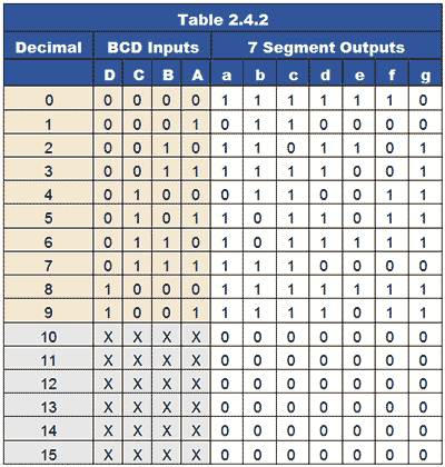
The truth table for a BCD to 7 segment decoder is shown in Table 2.4.2 and demonstrates the relationship between the four inputs ABC and D, and each of the display LEDs.
In columns a to g, an output of logic 1 lights one particular segment of the display. Logic 0 turns it off. An X output is called a ‘Don’t Care’ as it does not matter what the possible binary value would be in the BCD input columns A to D as they will not occur, (BCD will not produce values higher than 910 or 10012). The value of including these ‘Don’t Care’ outputs however, will be seen when working on the Karnaugh maps.
Notice that it is the convention to list the BCD input columns A to D in reverse order, making A represent the least significant digit and D, the most significant digit.
Designing a Decoder Circuit
The processes, and some of the choices to be made when using Karnaugh maps to minimise the digital circuits derived from complex truth tables such as Table 2.4.2 can be illustrated by creating a circuit to decode the 4 bit input to drive a single segment (segment ‘a’) of a 7 segment display. A similar process could be used to design circuits for each of the other six outputs b to g.
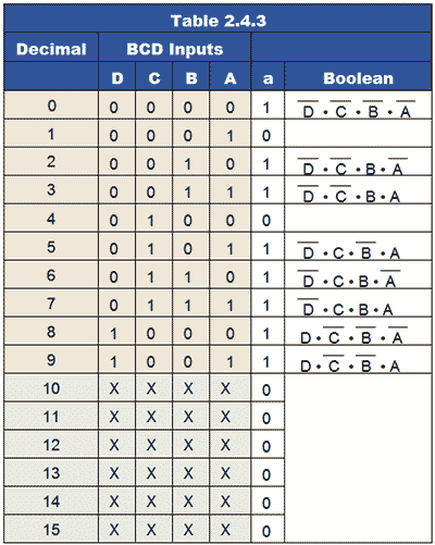
Table 2.4.3 illustrates the Boolean expressions derived from the BCD input columns that cause a logic 1 output at ‘a’.
Segment ‘a’ must be illuminated when any of the numbers 0,2,3,5,6,7,8 or 9 are present at the decoder inputs as a BCD value. Therefore 8 Boolean expressions are derived from Table 2.4.3, which will cause the decoder circuit to output logic 1 for these inputs.
The Boolean equation needed for the design of an appropriate circuit will therefore contain these 8 Boolean expressions, and so will be long and complex. It is therefore essential that such an equation is minimised, in order to make a practical circuit.
Decoder Minimisation Using Karnaugh Maps
The full Boolean formula for segment ‘a’ of the display, derived from Table 2.4.3 is:
a = (D • C • B • A) + (D • C • B • A) + (D • C • B • A) + (D • C • B • A) + (D • C • B • A ) + (D • C • B • A) + (D • C • B • A) + (D • C • B • A)
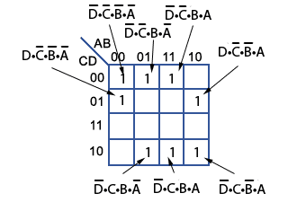
Fig. 2.4.6 Karnaugh Map Populated with Logic 1s
Each of the individual AND expressions in the formula are now used to populate a 16 cell (four input) Karnaugh map with logic 1s, corresponding with the cell values for A B C and D around the edges of the map, as shown in Fig. 2.4.6.
For example, the cell in the second row down, and the first column from the left contains a logic 1 that is labelled D•C•B•A corresponding to CD = 01 and AB = 00. Each logic 1 cell in the map is therefore equivalent to one of the Boolean expressions derived from Table 2.4.3. The complete Boolean formula for output ‘a’ is therefore contained in the Karnaugh map.
The logic 1 cells in the Karnaugh map can then be grouped as described in Simplifying Karnaugh Maps to produce minimal Boolean expressions as shown in Fig. 2.4.7.
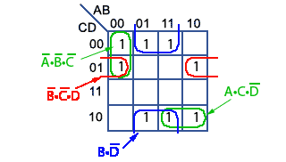
Fig. 2.4.7 Minimising the Karnaugh Map
In this example one group of four (in blue) has been found, containing:
(D • C • B • A) + (D • C • B • A) + (D • C • B • A) + (D • C • B • A)
This group follows the Karnaugh Map Rule 5 and the cells that DON’T change are B • D, so this group simplifies to B • D.
There is also a Karnaugh Map Rule 5 group of two (in red) containing:
(D • C • B • A) + (D • C • B • A)
This group also follows the Karnaugh Map Rule 5 and the cells that DON’T change are D • C • B, so this group simplifies to B • C • D.
Two further groups of two (green) simplify:
(D • C • B • A) + (D • C • B • A) to A • B • C
And:
(D • C • B • A) + (D • C • B • A) to A • C • D
This produces a simplified Boolean equation for output ‘a’ of:
a = (B • D) + (B • C • D) + (A • B • C) + (A • C • D)
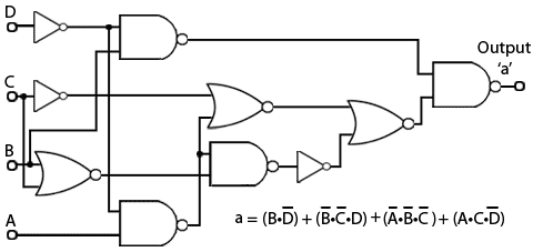
Fig. 2.4.8 Simplified Circuit for BCD to 7 Segment Decoder ‘a’ Output
This equation could be implemented as a circuit in a number of different ways, using AND OR and NOT gates, but Fig. 2.4.8 shows a circuit for the ‘a’ output, produced from the Karnaugh simplified equation, using NOT gates and the universal gates, NAND and NOR. Because there are not more than four of either NAND or NOR gates used, and less than 6 NOT gates, such a circuit would require one integrated circuit of each type, 3 in total.
However, although this circuit has been produced from a simplified Boolean equation, this does not automatically mean that the circuit is fully minimised, so may not yet be in its most economical form.
Using ‘Don’t Care’ Cells
The Karnaugh map in Fig. 2.4.7 used only logic 1s to make the simplified groups; if use is also made of the ‘don’t care’ cells, larger groups can be made, resulting in shorter Boolean expressions.
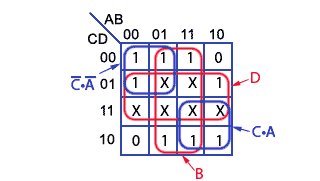
Fig. 2.4.9 Karnaugh Map with ‘Don’t Care’ Cells Included
Groups of one make 4 term expressions.
Groups of two make 3 term expressions.
Groups of four make 2 term expressions.
Groups of eight make 1 term expressions.
Including the ‘don’t care’ cells will not change the correct ‘a’ output of the resulting circuit, as although the input combinations creating these cells could (in pure binary) occur, in BCD, numbers greater than 10012 (910) can’t happen.
Fig. 2.4.9 shows the result of including the ‘don’t care’ cells in the groups. This allows two (red) 8 cell groups and two (blue) 4 cell groups to be made. The cells containing 0 are still ignored, as they do not produce the required logic 1 outputs. The map now results in a minimised, and therefore simpler Boolean equation than in Fig. 2.4.7. All relevant cells are now grouped using the maximum possible sizes for the groups, which results in a Boolean equation of:
a = B + D + (C • A) + (C • A)
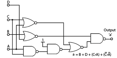
Fig. 2.4.10 Minimised Circuit for BCD to 7 Segment Decoder ‘a’ Output
This produces the circuit shown in Fig. 2.4.10, using only six gates instead of the ten required for Fig 2.4.8. The circuit now requires only two ICs. Additionally, as each gate has a finite propagation delay (the time from when the gate input becomes valid to the time when the output becomes valid), so the fewer gates there are between the circuit’s input and output, the faster the data can be processed. Notice that in Fig. 2.4.10 one of the NAND gates has one input connected permanently to logic 1 to convert it to a NOT gate, as described in Module 2.1. As there are four two input gates per chip, using a spare NAND gate in this way saves the use of a NOT IC.

Fig. 2.4.11 Grouping Zeros and ‘Don’t Cares’
A further option in simplifying circuits using Karnaugh maps is to produce a map grouping zeros instead of ones. Using the Karnaugh map produced from Table 2.4.3 again, if Zeros and ‘Don’t Cares’ are both included, this produces a map like that illustrated in Fig. 2.4.11.
The Boolean equation using zeros only, would produce:
a = (D • C • B • A) + (D • C • B • A)
but including the one available X (Don’t Care) produces a slightly simplified equation:
a = (C • B •A) + (D • C • B • A)
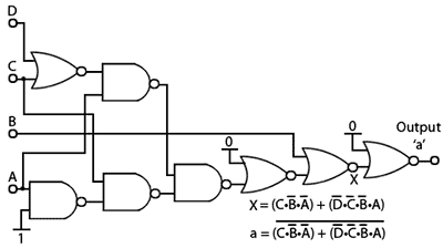
Fig. 2.4.12 Inverting the Output of a circuit Using Zeros
However this produces logic 1 outputs where ‘a’ was at logic 0 (for inputs 0001 and 0100 in Table 2.4.3). If this output is inverted however, the correct ‘a’ output according to the truth table for the decoder is produced. A circuit implementing this method is illustrated in Fig. 2.4.12. This circuit uses the same number of ICs as Fig. 2.4.10 but has a 50% longer propagation delay due to the extra gates used.
A circuit with a shorter propagation delay can be made, by using just the zeros in the Karnaugh map as shown in Fig. 2.4.13. This map contains only two 4-term groups but provides the opportunity to use two 4 input AND gates in the circuit illustrated in Fig. 2.4.14
This circuit again uses three ICs, a Hex inverter (with 6 NOT gates), a Dual 4 input AND and a Quad 2 input OR.
Because only two expressions are used the circuit is not minimised, but implemented as:
a = (D • C • B • A) + (D • C • B •A)
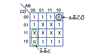
Fig. 2.4.13 Two Expression Karnaugh Map Using Zeros
In terms of propagation delay this circuit should be the fastest version of those discussed in this section, but the cost (based on average prices for 74 series ICs) would be approximately 30% more expensive than the cheapest. Clearly, in designing digital circuits there are choices the designer must make. Cost, speed, physical space and time to design are just some of the design considerations.
Relatively few new designs of medium to large systems will be implemented using 74 series ICs today. Now, large and complex Programmable Logic Devices will be used, where the actual logic functions within an integrated circuit, as well as the complex relationships between the functions are set by computer software, but for small scale and one-off designs, the low cost and reduced complexity of the 74 series chips is still valued.
Minimisation using Boolean algebra will largely be confined to simple circuits having few inputs, Karnaugh mapping being preferred as complexity increases. However both of these manual systems of circuit minimisation can be time consuming and error prone. Although Karnaugh mapping can theoretically handle circuits with up to six inputs, much work of this type can be better handled by computer based systems.
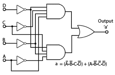
Fig. 2.4.14 Karnaugh Derived Faster Circuit Using Zeros


