

Google Ads
Module 2.4
Class A Amplifier Design
- After studying this section, you should be able to:
- • Carry out tests and modifications, and apply Negative Feedback to achieve specified performance criteria.
Part 4. Improving The Design.
Once the circuit has been through the initial stages of design, improvements can be made to get the design to match specific criteria. This design represents a basic audio amplifier, and therefore it should at least conform to the following very basic requirements. The gain (at the mid band frequency of 1kHz) should be of a specific value, this requirement would depend on the overall system design, of which this is only a single stage, but for this exercise:
Required Gain = 50
Bandwidth = 20Hz to 20kHz
Max. Undistorted Output Vpp > 70% of VCC
Achieving these criteria will require repeating the above design calculations and tests several times, because as you change one component in the design, some if not all of the test results previously obtained will change! Refining the design in this way is a normal part of any design process and learning how the different components change the operation of the whole circuit is a great learning exercise - enjoy!
Introducing some negative feedback.
In the DC only conditions introduced in Amplifiers Module 2.1, the gain of the amplifier was dependent on the ratio of RL to RE but when the emitter is decoupled by C3 in part 2, the AC voltage across RE is reduced to virtually zero by the low reactance of C3. This makes the ratio RL to RE just about infinite and the gain then becomes dependent on the hfe of the transistor. The hfe of small signal transistor is quite high, but also it can be seen from transistor data sheets to have a wide variation, 100 to 300 in the case of the 2N3904 .
Changing the transistor would therefore, very probably change the gain, also it would not be possible to make multiple versions of this design and expect the gain to be identical on each example. One way around these problems would be to use negative feedback. This will reduce the gain but make it much more dependent on fixed component values rather than the variable value of hfe.
Negative feedback also helps reduce distortion, and any background noise (hiss) generated within the circuit. It also helps to even out the gain over the amplifier’s bandwidth. If the gain is not constant, some frequencies will receive more or less amplification than others and ‘frequency distortion’ will occur. Slight differences in gain, of 1dB or less would not generally be noticeable, but using negative feedback can reduce larger differences.
Amplifiers Module 2.2 described how C3 is used to prevent negative feedback, but if some gain is sacrificed by allowing a controlled amount of negative feedback, this will flatten the response of the amplifier and increase the bandwidth, and although an increase in bandwidth may not be needed at this point, having achieved the advantages above, the bandwidth can be adjusted later.

Fig. 2.4.1 Two methods of applying NFB
There are two ways to reduce the decoupling effect of C3 as shown in Fig. 2.4.1 Both involve introducing an additional resistor RNFB into the emitter circuit.
In Fig. 2.4.1a RNFB is not decoupled.
In Fig. 2.4.1b RNFB reduces the decoupling effect of C3.
Adding RNFB reduces the decoupling effect of C3, making the (reduced) gain independent of hfe and sets it to the ratio of RL / RNFB. Once the value of RNFB has been calculated to give a gain AV of 50, the value of RE should also be re calculated and changed so that the original value of RE is shared between RE and RNFB. This will keep the DC conditions of the amplifier at about the same values as you set earlier.
Once these values have been calculated record the results in the Amplifier Design Record sheet, Part 4.1.
Because of the negative feedback, the effective input signal to the amplifier is reduced. This reduces Iin and because input current has input reduced, input impedance Zin (measured in Amplifiers Module 2.3) increase. The change in Zin will also affect calculations for the value of C1, so it would be good to re- check both the gain at 1kHz and the input impedance before carrying out the next operations. Record the new figure for Zin in the Amplifier Design Record sheet Part 4.1.
Refining the Bandwidth
The specification for this exercise asks for the bandwidth of the amplifier to be as close to the range 20Hz to 20kHz as possible, this part of the design exercise will adjust the high and low frequency limits of the bandwidth.

Fig. 2.4.2 Ideal Audio Response
Setting the low frequency limit of the bandwidth.
The low end of the bandwidth can be controlled by C1 and choosing an appropriate value allows the low frequency end of the bandwidth curve to be tailored to approximately (within the limits imposed by component preferred values) the frequency required e.g. −3dB at 20Hz.
C1 together with the input impedance (Zin) of the amplifier forms a high pass filter, which will shape the bandwidth at low frequencies. To get an accurate frequency for the -3dB point may require some experimentation with different preferred values of capacitor close to the calculated value, and repeated checks on the low end (20Hz) frequency of the bandwidth as described in Part 3 (5c). A suitable value for C1 can be found by re-arranging the standard formula for a filter corner frequency to give:
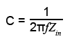
Calculate the value for C1 and the nearest preferred value and enter them in Part 4.2 of the Amplifier Design Record sheet.
The value of C2
The primary function of C2 is to provide DC isolation between this amplifier stage and any following circuitry, whilst coupling the AC signal. As such it needs to have a reactance that is low enough to pass all audio frequencies, a value of between 1µF and 10µF should be suitable. A more accurate value would only need to be considered if it would form any filter arrangement with any circuit connected to the output.
The value of C4
Now that the mid band gain and the low frequency limit of the bandwidth are set, C4 can be added to the circuit. The purpose of this capacitor is to form a low pass filter together with RL. This filter will control the high frequency limit of the amplifier reducing high frequency noise and instability. Too much gain at high frequencies can also lead to instability and positive feedback problems if not rejected. The value of C4 can be calculated in a similar way to the value for C1, however for C4, the resistive part of the filter is RL and the corner frequency of the filter (where the gain will drop by −3dB) will, for this exercise be 20kHz.
In a practical amplifier designed to accommodate all frequencies within the audio spectrum plus some higher frequencies to allow for the amplification of the audio harmonics the cut of frequency would be considerably higher, some commercial audio amplifiers will have a cut of frequency of around 100 to 150kHz.
The process of making C4 and RL act as a low pass filter is the same for any chosen frequency, only the corner frequency of the filter (your chosen cut off frequency) will be different, and so this will change the calculated value of C4. The main point is that you are able calculate the value of C4 to produce the cut off frequency of your choice. If you choose 20kHz you will loose some of the harmonics and the amplifier will not perform well at amplifying complex waves, such as square waves. If you choose a much higher value (or leave out C4 altogether, you run the risk of excessive HF noise and possibly some instability.
Calculate the value for C4 and the nearest preferred value and enter them in Part 4.2 of the Amplifier Design Record sheet
Maximum undistorted waveform
Apply a 1kHz sine wave to the amplifier input and connect an oscilloscope to the amplifier output to monitor the output waveform.
Adjust the amplitude of the input signal until the output wave observed on the oscilloscope just begins to show distortion.
Record the peak to peak value of the wave to ensure that VPP is greater than 70% of the value of VCC.