
Module 3.3
Logic IC Parameters
- After studying this section, you should be able to:
- Define 1 and 0 logic levels used in common logic families.
- • LSTTL.
- • HC/HCT.
- • ECL/PECL.
- Understand common terms relation to logic gates.
- • Noise Margin.
- • Minimising Power Consumption.
- • Sinking and Sourcing.
- • Fan out (AC and DC).
- Understand methods of interfacing between logic ICs.
- • Mixing Logic Families.
- • Logic Level Translation.

Fig. 3.3.1 Logic Levels
Logic 1 and Logic 0
Logic 1 and Logic 0 are not simply 5V and 0V or even Vcc and Ground. Within any family of ICs the voltages and currents indicating 1 and 0 cover defined ranges unique to that logic family. The range of voltages allowed for a particular logic level depends on the amount of current flowing into or out of the logic gate inputs or output, the larger the current the output is supplying, the lower the output voltage will be.
Each output will supply a certain amount of current before the output voltage falls too far to be called logic 1, and each gate input will need to be supplied with a certain amount of current to raise the input voltage sufficiently to be recognised as logic 1.
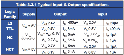
Examples of typical logic levels at inputs and outputs in a range of logic families are illustrated in Fig. 3.3.1. These levels are fairly standard throughout a particular family, although there can be minor differences in these and other parameters, between products from different manufacturers. In addition there are sub families within these families that may have different defined levels. When designing digital circuits, or replacing ICs in critical equipment, it is therefore essential to consult the appropriate manufacturer’s data sheets.
Logic 1 levels for inputs and outputs are shown in red and logic 0 in green. To highlight the fact that true ECL gates, have negative logic levels, these colours have been changed to yellow and blue respectively.
Notice that the logic levels for outputs (left column) and inputs (right column) in all of the families are different. This ensures that provided that the output voltage of a gate is within its defined logic limits for 1 or 0, any compatible gate input connected to that output will recognise the correct 1 or 0 levels. The difference between levels at the output and input in any particular family is called the ‘Noise Margin’.

Fig. 3.3.2 Logic IC Decoupling
Noise Margin
Because voltages in digital circuits can be continually changing very rapidly between logic 1 and logic 0, (virtually between supply voltage and ground), they have the potential to produce a lot of noise, in the form of high frequency voltage spikes on the IC power supply lines.
To counteract this it is important to include effective decoupling, not only at the power supply unit, but also by connecting decoupling capacitors across the VDD and 0V connections at each IC. These capacitors are normally connected as physically close to the IC as possible, as shown in Fig. 3.3.2.

Fig. 3.3.3 Noise Margin
Despite these measures, it is possible that some noise will remain that could disturb the logic levels of digital signals. However logic ICs have a built in ‘Noise Margin’, illustrated in Fig. 3.3.3, This is the difference between the worst-case voltage ( VOH) for logic 1 at the output , which is 2.4V in the case of 74HCT, and the minimum voltage required for logic 1 to be recognised at the input (VIH), 2.0V in 74HCT. This difference (0.4V) should be enough to ensure that noise does not cause a wrong logic level to be seen by the 74HCT input; a similar noise margin is provided for logic 0 (VIL−VOL) as shown in Fig. 3.3.3.
It can be seen from Fig. 3.3.1 that different logic families have very different noise margins. The CMOS 74HC gates have a much wider noise margin than LS TTL or the TTL compatible 74HCT series, making them much more tolerant of noise. This is because the CMOS outputs are normally driven very close to VDD or 0V as very little current is drawn from a CMOS output to drive any CMOS inputs connected to it.
Minimising Power Consumption
In both CMOS and TTL ranges it is important that the central (white) range of voltages in Fig. 3.3.1 is avoided as much as possible. This is done by ensuring that switching between 1 and 0 is as fast as possible. If the IC is operating within the ‘invalid range’, power consumption increases dramatically. When the output voltage is close to the supply voltage, current is almost zero and therefore power (V x I) is very low. Similarly when the output is close to 0V but maximum current is flowing, V x I is again very low. Power consumption is at its highest when both voltage and current are around the mid range, and operating the ICs in this range would substantially increase the heat dissipated by the IC.
However, any unused inputs on CMOS ICs will tend to float to a mid voltage level, causing power dissipation to increase. To avoid problems with floating CMOS inputs, they should therefore be connected to either supply or ground, either directly or via a resistor, so they are not allowed to ‘float’ and cause excessive power consumption. This is not absolutely necessary, (though good practice), with TTL ICs as any unused TTL inputs will float up to logic 1.
Notice that ECL/PECL gates operate exclusively in this mid range area; this is why power consumption in these families is higher than in TTL or CMOS. However the close proximity of the logic 1 and logic 0 values in ECL allows for much higher switching speeds. This operation also gives ECL a much narrower noise margin however, making these chips more susceptible to noise. This is the reason for ECL having its positive supply tied to 0V, which is generally less noisy than sharing a positive supply with many other ICs.
Mixing Logic Families
The differences in the output voltage and/or current levels for TTL and the CMOS gates can affect circuit operation if both bipolar and CMOS logic families are used in the same circuit (e.g. LS TTL and HCT or CMOS), or if an older TTL IC is replaced by an ‘equivalent’ HCT chip during repairs or upgrading.
When mixing logic families it is important to consult input and output specifications such as those listed in Table 3.3.1 to ensure that the input and output conditions are compatible. The data in Table 3.3.1 shows typical input and output values for logic families, but particular ICs within a family or sub-family, and ICs from different suppliers will differ. The only way to be sure of complete compatibility is to consult the manufacturers data sheets for the ICs concerned.
Generally TTL outputs will interface to other TTL family inputs, and to 74HCT, which has TTL level inputs and CMOS level outputs.
The 74HCT outputs will interface to CMOS inputs provided both ICs are working from a common +VDD supply. This should not be a problem with the 74HC series, as it will operate on 5V supplies.

Fig. 3.3.4 Interfacing TTL to 74HC
Connecting a TTL output to a CMOS HC input may work if TTL input is not heavily loaded. A problem occurs however when more current is sourced by the TTL logic 1 output. Its output voltage (VOH) depends on the current being drawn from it and will vary from around 3.3V with no load current, down to about 2.4V when the output is sourcing around 400µA. As the HC gate input requires a minimum input voltage (VIH) of 3.2V there is a chance that at some output current between 0 and 400µA the TTL output will fall below 3.2V, and fail to be recognised as logic 1 by an HC input using its maximum supply voltage of 16V. Even if the HC supply is reduced to 4.5V there will still be a chance of mismatch.
The remedy is to fit a pull up resistor from the TTL output to Vcc as shown in Fig 3.3.4, which will increase the TTL output voltage (VOH) sufficiently to ensure correct interfacing. The value of the resistor should be between 1K and 2K ohms, the optimum value depending on the Fan out factor of the TTL gate and the number of gates being driven, the less current the output is sourcing, the lower the value of pull-up resistor needed.
Level Translation
With the older +5V TTL and +3V to +18V 4000 CMOS families the logic levels must be shifted considerably. For this purpose, a level translator IC such as the MC14504B from ON Semiconductor will provide level shifting for up to six ICs with VCC or VDD at any value between +0.5V and +18V. An alternative solution to level translation is to use Open Collector ICs.
ECL to TTL interfacing is carried out by ICs such as the MC10ELT25 from ON Semiconductor.
Sinking and Sourcing

Fig.3.3.5 Sinking and Sourcing
Because the output circuits of logic gates are a type of push-pull or ‘Totem Pole’ output with only one of its two output transistors conducting at any one time, when the output terminal is at logic 1 T4 is turned on the output terminal of Gate 1 will supply (or SOURCE) current via T4 and D1 to the input of Gate 2. This will cause gate 2 input to also be at its logic 1 state as shown in Fig. 3.3.5 (a).
When gate 1 output is at logic 0, T4 is turned off and T3 is turned on, and output current will now flow in the opposite direction, from the input of Gate 2 in Fig 3.3.5 (b) and via T3 collector and emitter to ground; this is called SINKING the current.
When a LS TTL gate output acts as a source, a maximum source current of -400µA is available to be drawn from the output terminal. Note that the minus sign used in this case signifies a current that is flowing FROM the gate output. When the output is sinking current, the LS TTL gate is able to sink 8mA. Notice the sink current has no minus sign as it flows into the output terminal.
Fan Out
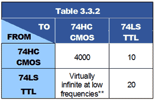
A standard LS TTL gate is therefore able to sink 20 times the amount of current it is able to source. This ratio between sinking and sourcing current is typical with bipolar gates. The above conditions mean that the output of a standard LS TTL gate is capable of driving up to 20 LS TTL inputs without its output voltage falling below the minimum specified for logic 1. This is described as a FAN OUT FACTOR of 20, but each logic family has its own particular ratio of sinking to sourcing currents, so the fan out factor of 20 is only correct where a standard LS TTL gate is driving one or more gates of the same (LS TTL) family.
Because gates of other families have different input and output currents the actual fan out factor will be different when logic families are mixed within a circuit. For example, Table 3.3.2 shows how mixing LS TTL and CMOS HC gates affects their fan out factors.
A 74HC output can feed up to 4000 74HC inputs, because the input currents of 74HC gates are extremely low, but only 10 74LS TTL inputs.
A Standard LS TTL gate output can drive up to 20 LS TTL inputs, but one LS TTL gate output can drive a virtually infinite number of 74HC CMOS gates because of the low current requirement of 74HC CMOS gates.
High Frequency AC Fan Out **
However, although a standard LS TTL output will apparently feed an infinite number of 74HC inputs (** in Table 3.3.2), when high frequency signals are used, additional limits need to be considered. Each CMOS input and output has a capacitance of several pF, and if a CMOS output is to feed a number of inputs, the individual input capacitances are in effect connected in parallel (and so add) to form a larger capacitance across any output driving the CMOS inputs.
The effect of this capacitance, as well as any capacitance due to connecting lines on the printed circuit board will combine with the output impedance of the gate to form a low pass filter. The effect of this filter will be to remove some of the higher frequencies in the signal, increasing rise and fall times, lengthening propagation delay and potentially causing timing errors in the system, therefore large fan outs are best avoided. These effects make the design of high-speed digital systems similar in some respects to high frequency RF circuits where stray capacitance, cable routing and interference play a large part in the circuit design.