Module 3.2
How Logic Gates Work
- After studying this section, you should be able to:
- Understand How Logic gates Work.
- • CMOS, TTL and ECL.
- • Supply voltages.
- • Propagation delay.
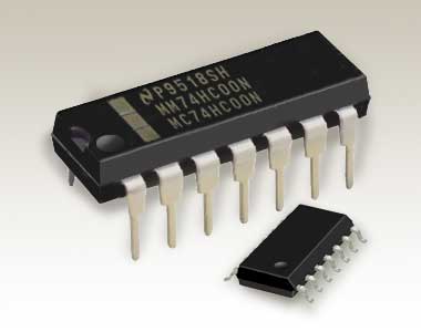
Fig 3.2.1 Typical Logic IC Packages
Logic Technologies
Small and medium scale (SSI and MSI) Logic IC families are currently made in a wide range of sub-families and a variety of package types, using three basically different technologies:
• TTL (Transistor Transistor Logic)
• CMOS (Complimentary Metal Oxide Semiconductor)
• ECL (Emitter Coupled Logic)
Transistor Transistor Logic (TTL)
TTL gates use a 5V(±0.25V) supply, and are capable of high-speed operation. Over 600 different logic ICs are available, covering a very wide range of digital functions. Due to the use of bipolar transistors, TTL has much higher power consumption than similar CMOS types, when working at relatively low frequencies. As the frequency of signals handled increases however, this difference decreases as the power consumption of CMOS increases and TTL power consumption remains nearly constant.
TTL NAND Gate Operation
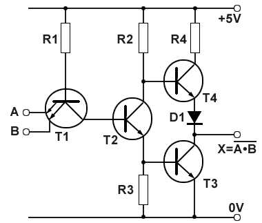
Fig. 3.2.2 Schematic diagram of a TTL NAND Gate
Notice that this circuit looks similar to those found in analogue push pull amplifiers, except that the transistors here are driven either into cut-off or saturation, rather than working in their linear operating condition. Also, being constucted within an IC, it can use a device not normally found in conventional analogue amplifiers, a multi emitter transistor.
Fig. 3.2.2 shows a typical schematic for a TTL NAND gate. R1 is a low value resistor (about 4K) and as the base current of T1 is small, the base voltage is about +5V. If both emitters of T1 are at logic 1, (also around +5V), there will be very little potential difference between base and emitter, and T1 will be turned off. As T1 is not conducting, its collector will also be at about 5V, and due to this high potential, T2 base will have a higher potential than its emitter, which will cause T2 to conduct heavily and go into saturation.
T2 collector will therefore fall to a low potential, and the emitter voltage of T2 will rise due to the current flow through R3. The voltage across R3 will rise to a sufficient level (about 0.7V) to fully turn on T3. As T3 saturates, its collector voltage will fall to about 0.2V, thus giving a logic 0 state at the output terminal.
T4 emitter voltage is made up of T3 VCE (about 0.2V) plus the forward voltage drop across D1, which will be about 0.7V, giving an emitter potential of 0.2V + 0.7V = 0.9V, the same as its base voltage.
The base potential of T4 is made up of T3 base/emitter potential VBE (about 0.7V), plus the collector/emitter, potential (VCE) of T2, (about 0.2V), giving a base voltage for T4 of about 0.9V. Therefore the base and emitter voltages on T4 are approximately equal, so T4 will be turned off.
With BOTH input terminals are at logic 1 therefore, the output terminal will be at logic 0, the correct operation for a NAND gate.
If either one of the inputs is taken to logic 0 however, this will make T1 conduct, as the emitter that is at logic 0 will be at a lower voltage than that supplied to the base by R1. This will cause T1 to saturate, taking its collector to a low potential (less than 0.8V) and as this is also connected to T2 base T2 will turn off, making its collector voltage and T4 base voltage, rise to very nearly +Vcc.
As virtually no current (ICE) is flowing through T2 collector/emitter circuit, practically no voltage is developed across the emitter resistor R3, reducing T3 base voltage to 0V, and so T3 is turned off. However, sufficient current will be flowing out of the output terminal (feeding the next gate input circuit) to cause T4 emitter to be held at about 4.1V. This is 0.9V below +Vcc, made up of the voltage across D1 (0.7V) plus the saturation voltage VCE of T4 (0.2V). This places about 4V or logic 1 (between 2.4V and 5V) on the output terminal.
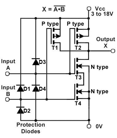
Fig. 3.2.3 CMOS NAND Gate
Complimentary Metal Oxide Semiconductor (CMOS)
CMOS ICs can operate from a wide range of supply voltages (typically 3 to 18V, and lower with some sub families), with very low power consumption. The name CMOS (COMPLIMENTARY Metal Oxide Semiconductor) is used because opposite types, both P type and N type MOSFETs are used in the construction of these gates. Fig 3.2.3 shows a theoretical schematic circuit for a NAND gate.
CMOS NAND Gate Operation
T1 and T2 are P channel MOSFETs and either of these transistors will be turned on when logic 0 is applied to its gate. T3 and T4 are N channel MOSFETs and either of these transistors will be turned on by applying a logic 1 to its gate.
T1 and T2 are connected in parallel from supply to the output X, so switching either of them on will result in a logic 1 at output X.
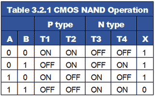
T3 and T4 are connected in series between X and ground so when both are switched on, a logic 0 will appear at output X. The eventual logic state at X depends of course on the on or off state of the combination of all four transistors, and these are controlled by the logic states applied to the inputs A and B as can be seen in Table 3.2.1.
Input A controls T2 and T3 so that when logic 0 is applied, T2 is on and T3 is off. Logic 1 on input A reverses this condition.
Input B controls T1 and T4 so that logic 0 applied to B turns T1 on and T4 off. Logic 1 on input B reverses the condition.
Anti-Static Protection
Because MOSFETs, have a gate that is insulated from the transistor’s conducting channel, they can also be called Insulated Gate Field Effect Transistors (IGFETs) and have practically no current flowing into their inputs, therefore any high voltages due to static electricity are not reduced by current flow so can easily destroy the very thin insulating layer between the gate and the conducting channel of the transistor. To minimise such damage and protect the gates from any high voltage static electricity spikes that may appear across the IC during handling, CMOS ICs should always be stored in anti static packaging, and handled in accordance with manufacturers handling procedures.
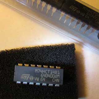
Fig. 3.2.4 Anti Static Packaging
To protect the ICs from high voltage spikes when in circuit, protection diodes (see Fig. 3.2.3) are used at the gate inputs. Protection diode D3 is connected between input A and +Vcc so that if any voltage higher than Vcc appears at input A, D3 will become forward biased and conduct, limiting the input voltage to +Vcc.
Similarly, if a negative voltage appears at input A, D4 will conduct, limiting the input voltage to no less than 0V.
Input B is protected in a similar manner by D1 and D2. Note however, that although the diodes offer protection, it is still possible that very large static voltages may still damage these devices, so anti-static precautions should always be used when handling CMOS devices.
Capacitance in CMOS devices
Because CMOS transistors are IGFETs with insulating layers between electrodes, they naturally act as capacitors. The value of these capacitors is of course small because the electrodes either side of the insulating layer are extremely small. However the combined capacitance between the various sections of the several IGFETs that make up a CMOS gate, added to any capacitance between lead-out wires etc. is sufficient to have an effect on the overall gate performance. When a change in logic state occurs, ideally it should complete its transition from 0 to 1, or 1 to 0 immediately. However because of the gate capacitance and internal resistances that are present, the change cannot happen in less time than the CR time constant of the circuit. The output of a gate cannot complete its change until the input has completed its transition, and the output must similarly take some additional time, before reaching its new value.
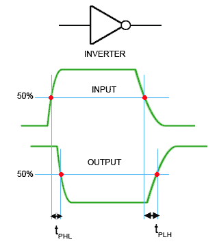
Fig. 3.2.5 Propagation Delay
Propagation Delay
Any gate introduces some delay between when its input changes and when a resulting change takes place at its output. This is called the propagation delay of the gate, and is made up of two, often different delays, as shown in Fig. 3.2.5 using a simple inverter gate as an example.
The High to Low Propagation Time (tPHL) is measured from the time (usually in nanoseconds) when the input rises past the 50% level, to the time when the output falls past the 50% level. A similar, but usually longer delay (tPLH) is measured from when the input falls past the 50% level, to when the output rises past the 50% level. Therefore the average propagation delay of the gate is:
(tPHL + tPLH) / 2
Typical average propagation delay for a 74HC04 inverter is about 8ns.
Emitter Coupled Logic (ECL)
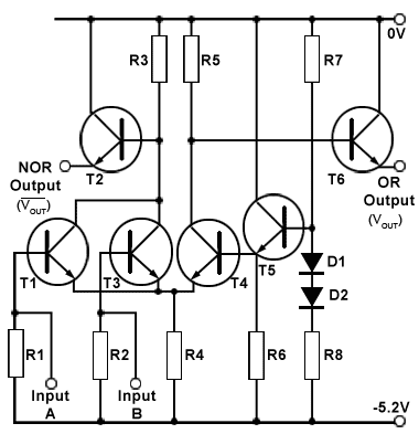
Fig. 3.2.6 ECL OR/NOR Gate
Because the early designs of ECL ICs needed a negative supply voltage of -5.2V they were not particularly compatible with either CMOS or TTL circuits, even though, like TTL, they use bipolar transistors. However there are now newer ECL sub families available that use positive supplies such as PECL (+5V) and LVPECL (+3.3V). Although the supply voltages for these ECL gates are now more compatible with CMOS and TTL, the logic levels used in ECL are quite different to other logic families. ECL is extremely fast in operation with propagation delays of less than 1 nanosecond available.
ECL was extensively used in early super computers, but because of its high power requirement (up to 40mW per gate) fell out of general use. Today modern ECL sub families such as PECL or LVPECL are now mainly used for interfacing CMOS or TTL digital systems to high frequency signal communication (up to several GHz) circuits. The two opposite logic state outputs (VOUT and VOUT) means that the ECL OR gate illustrated in Fig. 3.2.6 can operate as an OR gate or a NOR gate and also makes ECL ideal for interfacing with differential (two conductor) transmission lines possible. This method of transferring high speed digital data uses a pair of high frequency anti-phase signals as a method of cancelling out electromagnetic interference that may be picked up during transmission.
Operation
The basis of the ECL circuit is a differential amplifier (T3 and T4 in Fig. 3.2.6), which is ideal for high frequency use and reducing noise on the amplified signals. This amplifier compares the voltage at the inputs (the bases of T1 and T3) with a steady reference voltage produced by T5, D1 and D2. To avoid any delay caused by the transistors saturating, the differential amplifier is designed to always be in a linear amplifying mode, approximately half way between saturation and cut off.
The voltage change between logic 1 and logic 0 is between −0.9 and −1.75 respectively. Power consumption is considerably higher than CMOS or TTL because the transistors in the differential amplifier are always conducting, rather than switching on and off as in TTL and CMOS.
ECL and PECL use differential transmission, a pair of conductors with opposite polarity signals, along which data can be transmitted for around 50m. The technique reduces interference in the transmission lines when passing data from one digital system to another, and was used in many data transmission links in computing up to the 1990s, but for many uses, such as USB, HDMI etc. ECL has now been largely superseded by LVDS (Low Voltage Differential Signalling), a CMOS based high frequency digital transmission system. This system uses much less power than ECL and can transfer data over distances of up to 10m at a rate of several hundred Megabits per second.


