Module 5.7
Registers
- After studying this section, you should be able to:
- Understand the operation of digital parallel in/parallel out (PIPO) registers.
- Describe the action of serial and parallel shift registers.
- • Serial in/Serial out (SISO).
- • Serial in/Parallel out (SIPO).
- • Parallel in/Serial out PISO.
- Understand the operation of reversible shift registers.
- Recognise common features used in shift register ICs.
- Use Software to analyse the operation of shift registers.
Parallel In - Parallel Out (PIPO) Registers
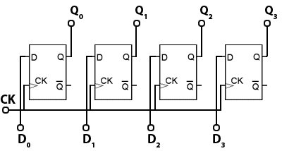
An electronic register is a form of memory that uses a series of flip-flops to store the individual bits of a binary word, such as a byte (8 bits) of data. The length of the stored binary word depends on the number of flip-flops that make up the register. A simple 4-bit register is illustrated in Fig. 5.7.1 and consists of four D Type flip-flops, sharing a common clock input, providing synchronous operation ensuring all bits are stored at exactly the same time.
The binary word to be stored is applied to the four D inputs and is remembered by the flip-flops at the rising edge of the next clock (CK) pulse. The stored data can then be read from the Q outputs at any time, as long as power is maintained, or until a change of data on the D inputs is stored by a further clock pulse, which overwrites the previous data.
Different types of register are generally classified by the method of storage and readout used; this basic form of register is therefore classified as a ‘Parallel In/Parallel Out’ (PIPO) register.
Shift Registers.
Shift registers have a similar structure to the PIPO register but have the added ability to shift the stored binary word left or right, one bit at a time. This makes them extremely useful for many applications. They are used in handling serial data and converting it to parallel form or back again to serial form, and therefore are an essential component in communication systems. Shift registers are also essential in arithmetic circuits where binary numbers may be shifted right (and so divided by two), or left (multiplied by two) as part of a calculation. Shift registers can be used to delay the passage of data at a particular point in a circuit. As the data is shifted one bit at a time from input to output, the amount of delay will depend on the number of flip-flops in the register and the frequency of the clock pulses driving the shift register. Because a number of serial bits of data are stored as they enter the input, and are then recovered from the output at some later time, this action can also be described as a serial memory, or as a digital delay line.
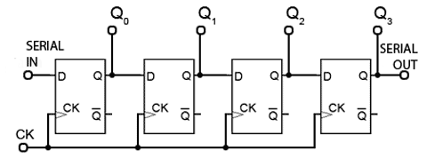
The simple storage register shown in Fig. 5.7.1 can be modified to a shift register by connecting the output of one flip-flop into the input of the next, as shown in Fig. 5.7.2. The basis of shift register circuits is the D-type flip-flop, but the clocked SR or the JK flip-flop may also be converted to D-types by the inclusion of an inverter between S and R or between J and K. In all cases the clock input is in synchronous mode.
The serial input of the shift register in Fig. 5.7.2 is the D input of the first flip-flop, and the serial output is the Q output of the last flip-flop in the chain. The logic state at the serial input appears at the output, a number of clock pulses (equal to the number of flip flops) later.
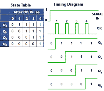
Fig. 5.7.3 Timing Diagram and State Table for SISO Operation
Modes of Shift Register Operation.
SISO
A State Table and Timing Diagram illustrating the operation of Fig.5.7.2 is shown in Fig. 5.7.3 where the timing diagram shows the time relationship between the CK pulses and changes at the Q outputs of the circuit. It can be seen that if the serial input goes from 0 to 1 just before CK pulse 1, the Q output of flip-flop FF0 will go high at the rising edge of CK pulse 1. At the next clock pulse rising edge, the logic 1 will be transferred to FF1 and so on until it reaches FF3, and the serial output.
The same action can also be illustrated by a State Table, which, rather than showing timing data, shows the states of the four Q outputs after each clock pulse. After each CK pulse one more flip-flop output is set to 1 until, after 4 pulses, column 4 shows that all Q outputs, including the serial output, are at logic 1. This form of operation is called ‘serial in/serial out’ or SISO.
SIPO
In Fig. 5.7.4 the shift register is modified to include additional Q outputs from each flip-flop, so allowing the register to input serial data, and output it in both serial and parallel form. The register could therefore now be called both a ‘Serial In/Serial Out and Serial In/Parallel Out’ (SISO/SIPO) register. This format is the basis for converting serial data to parallel data.
PISO
If use is also made of the Q output, and the additional preset (PR) and clear (CLR) inputs available on many flip-flops, the shift register could be made more versatile still.
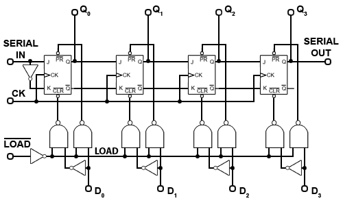
Fig. 5.7.5 shows a shift register modified to enable it to be loaded with a 4-bit parallel number, which may then be shifted right to appear at the serial output one bit at a time. As the ‘Parallel In/Serial Out’ or PISO register also has a serial input, it can also be used as a SISO register, and if extra outputs from each Q output were also included, the register would also have Serial In/Parallel Out (SIPO) operation.
Loading Parallel Data
If the LOAD input is taken to logic 0, the LOAD control line connected to the four pairs of NAND gates associated with the four flip-flops will be at logic 1, and all four pairs of NAND gates will be enabled. Therefore a logic 1 appearing on any of the D inputs will be inverted by the NOT gate connected to the D input, making the inputs to the left hand NAND gate of the relevant pair of gates, logic 1 and logic 0. This will cause logic 1 to be applied to the CLR input of the flip-flop.
The right hand NAND gate of the pair will have both inputs at logic 1, due to the logic 1 on LOAD line and logic 1 on the D input, and so will output logic 0 (NAND gate rules) to the PR input of the flip-flop, setting the Q output to logic 1.
If the D input is at logic 0, the left hand gate of the NAND gate pair will output logic 0 and the right hand NAND gate will output logic 1, causing the CLR input to clear the Q output of the relevant flip-flop to logic 0.
Notice that as JK flip-flops are being used in this design, a NOT gate is connected between J and K of the first flip-flop of the chain to make the JK flip-flop mimic a D Type. The remaining flip-flops of the shift register have J and K connected to the previous Q and Q outputs, so will also be at opposite logic states.
A 4-bit reversible shift register.
The shift register in Fig 5.7.5 could be operated as:
- A parallel in/parallel out register. (PIPO)
- A Serial in/serial out register. (SISO)
- A serial in/parallel out register. (SIPO)
- A parallel in/serial out register. (PISO)
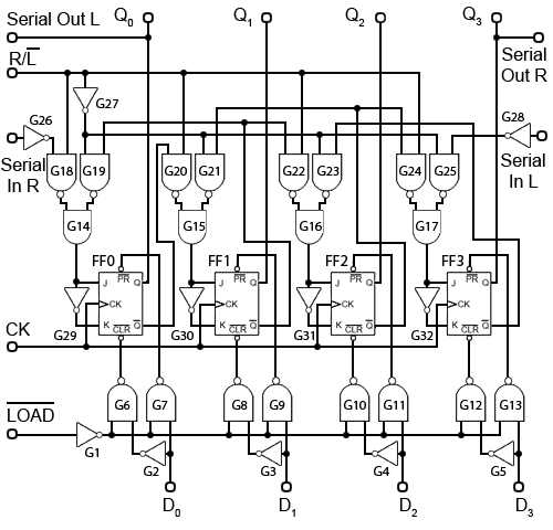
However Fig 5.7.5 can only shift data in one direction, i.e. left to right. To be truly versatile it could be an advantage to be able to shift data in both directions and in any of the four shift register operating modes. Fig. 5.7.6 achieves this by adding data steering circuitry.
The gating arrangement at the bottom of Fig 5.7.6 (gates G1 to G13) is exactly the same as that described above in Fig. 5.7.5, and these gates control the loading of parallel data.
Gates G14 to G28 in Fig 5.7.6 control the direction of data flow through the register. The JK flip-flops use the inverter gates G29 to G32 to ensure that J and K are at opposite logic states, so the flip-flops are mimicking D Type operation, with J being used as the data input. Notice also that the clock is connected in the familiar synchronous mode.
Operation.
In any of the modes involving serial operation, data may be shifted left or shifted right by the application of a suitable logic level at the shift control (R/L) input.
With a logic 1 at this input the register is in the shift right mode, and data is taken into the ‘Serial in R’ input to be shifted right by application of successive clock pulses, appearing as parallel data, changing with each clock pulse, on the flip flop Q outputs. After four clock pulses the data begins to appear in serial form on the Q3 output, which is also the ‘Serial Out R’ output.
The logic 1 on the shift control (R/L) enables gates G18, 20, 22 & 24, but because the logic 1 is inverted by G27, gates G19, 21, 23 & 25 are disabled.
The path of serial data (e.g. a logic 1) from left to right is as follows; the logic 1 appearing at the input to G26 is inverted and passes through G18 which re-inverts it to logic 1 and, as G19 is disabled its output must also be at logic 1. Both inputs to the AND gate G14 are at logic 1 and therefore so is its output, (AND gate rules) making the J input of FF0 logic 1.
On the arrival of a clock pulse, the logic 1 input to FF0 will appear on the output Q0. Its inverse (logic 0) will also appear on the Q output of FF0. This logic 0 forms the input to the next multiplexer arrangement, gates G20, 21 & 15. As G20 is enabled (and G21 disabled) the logic 0 becomes logic 1 at G15 output and so is fed to the J input of FF1. This method is used to transfer data to each flip-flop in the chain.
To achieve shift left operation, the shift control (R/L) is set to logic 0 and so enables gates G19, 21, 23 & 25 while disabling gates G18, 20, 22 & 24. Therefore the Q output of FF3 is connected via G23 and G16 to the D input of FF2, the Q output of FF2 is connected to the J input of FF1 via G21 and G15 (remember that G24 is disabled, so FF3 is isolated from this path). Finally, the Q output of FF1 is connected via G19 and G14 to the J input of FF0, the Q0 output of which is also the ‘Serial Out L’ output. The ability to shift data in either direction, together with the parallel input and output facilities make this register a very versatile device.
It is common to connect shift register ICs in cascade, using the serial output of one register to connect to the serial input of the next register in the chain. For this reason both the data and clock inputs and outputs of register ICs are normally buffered.
Some examples from the many commercially available IC registers using these and similar methods, available in both CMOS and TTL versions, are listed below.
- 74HC164 8-Bit SIPO Shift register from NXP
- 74HC594 8-Bit SIPO/SISO with PIPO output storage register and dual clocks - from NXP.
- 74HC595 8-Bit SIPO/SISO with tri-state output PIPO storage register and dual clocks - from NXP.
- HEF4014B PISO Register with 8-bit synchronous parallel LOAD and outputs from Q5, Q6 & Q7 only - from NXP.
- CD4031B 64 Stage SISO shift register with re-circulation mode - from Texas Instruments.


