Module 3.4
Special Purpose Logic ICs
- After studying this section, you should be able to:
- Understand the need for Special Purpose Logic ICs.
- • Wired AND/OR Logic.
- • Open Collector Gates.
- • Negative Logic.
- • Schmitt Gates.
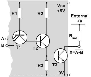
Fig. 3.4.1 Simplified circuit of an Open Collector NAND Gate
Open Collector Gates
Fig. 3.4.1 shows the internal circuit of an open collector NAND gate. The grey area illustrates a single gate within an IC. Instead of the normal Totem Pole output stage, the single output transistor T3 has its collector brought out to an external pin, which can be connected to an external power supply, at a different voltage to the VCC supply of the IC, via an external load resistor REXT.
In Fig. 3.4.1, when both inputs A and B are at logic 0, the high voltage applied to T1 base will cause it to turn on, so that T1 collector will go to near 0V and T2 will turn off.
As T2 is off there will be virtually no current through R3 so the voltage at T3 gate will be around 0V. T3 will therefore be turned off and the external pull up resistor REXT will pull the collector voltage of T3 up to +V, which will be at the valid logic 1 level of the next gate.
Logic Level Translation
Open collector and open drain gates can therefore be used for changing the levels of an output to match the higher or lower logic levels of an input on a different family of gates, when gates of mixed families are used.
Open collector gates can be used with external collector VCC supplies having a voltage typically somewhere between +1.5V to +5.5V for logic gates, Buffer ICs are also available that can operate on collector VCC supplies up to +30V. The maximum value of collector voltage is set by the VOH parameter of the open collector gate.
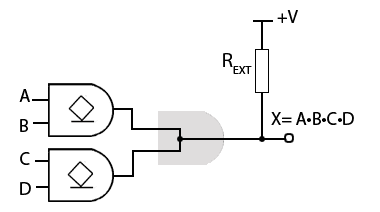
Fig 3.4.2 Wired AND Function
Wired Logic Functions
Open collector ICs are available in most of the logic types, AND, NAND etc, with the exception of OR gates. However open collector gates can be used to make both wired AND and wired OR functions as shown in Figs. 3.4.2 and 3.4.3. The outputs of gates without open collectors must not be connected together, because if the outputs happen to be at opposite logic states, the gate with a logic 0 output will try to sink more current than the logic 1 gate can source, and damage will most probably occur. However with open collector (or drain) gates, a gate output at logic 0 will be sinking current drawn from the external pull up resistor REXT, and any other connected open collector gate trying to output a logic 1 will have its output transistor turned off and so will not be sourcing any current.
Wired AND
If two or more open collector gate outputs are connected together, any gate with a logic 0 output will pull all other connected outputs to logic 0, giving an output of logic 0 at output X, but if all the connected outputs are at logic 1, then X will be at logic 1, the action of an ‘invisible’ AND gate.
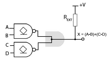
Fig 3.4.3 Wired OR Function
Wired OR
It is also possible to implement a wired OR function using open collector (or drain) gates as shown in Fig. 3.4.3, although the explanation here is a little more complex as it involves using Negative Logic.
The circuit in Fig. 3.4.3 is used to obtain the Boolean function (A•B)+(C•D) without using a physical OR gate.
Notice that the circuit in Fig. 3.4.3 is similar to the wired AND circuit in Fig. 3.4.2, except that the two open collector AND gates have been replaced by two open collector NAND gates. The main difference with this circuit however is that to obtain an OR function from what appears to be a wired AND function, Negative Logic is applied.
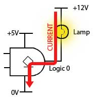
Fig 3.4.4 Active Zero
Negative Logic
In Digital Electronics it is usual to explain the operation of a circuit theoretically in terms of 1 and 0, but the actual gates are really just specialised analogue circuits. As explained in Module 3.3, the outputs normally thought of as 1s and 0s are really ranges of voltage and current, 1 and 0 are no more than convenient names given to these voltages and currents. It is also usually assumed that logic 1 refers to the higher of the two voltage ranges − but that need not be so! Also logic 1 is normally the active state of an output, and logic 0 is the inactive state, but this is not always what is required.
The source current available from an open collector gate output when it is at logic 1 is very small, compared to the current the gate will sink when its output transistor is turned on, giving an output of logic 0.
It is quite reasonable therefore, to drive some output device, such as a lamp or relay for example, using the higher current available from a logic 0 output, as shown in Fig. 3.4.4.
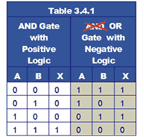
In negative logic it is assumed that the active state is the low voltage state and that this is called logic 1. What this does to the familiar truth tables used in positive logic is to replace all the logic 1s (previously assumed to be the active state) with logic 0s and vice versa.
The effect of this reversal of logic states can be seen in Table 3.4.1. The X column for the positive AND gate is as would be expected; a logic 1 when both A and B are 1, otherwise logic 0s. However using negative logic on the same physical AND gate, simply swapping the 1s and 0s in both the input and output columns has changed the X output column from three 0s and a 1, to three 1s and a 0, so that X = 1 whenever A or B is 1. The AND gate has been transformed to an OR gate!
Using negative logic will change the function of any of the six two input logic gates, if you want to see what happens, try re-writing the truth tables for AND, OR, NAND, NOR, XOR, and XNOR in a similar manner to Table 3.4.1. However, negative logic is not widely used and so unless a logic circuit is actually described as using negative logic, it can be assumed that positive logic is being applied.
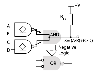
Fig. 3.4.5 How the Wired OR Circuit Works
Negative Logic and the Wired OR Circuit
Fig. 3.4.5 shows how the wired AND circuit shown in Fig. 3.4.2 is made to work as the wired OR in Fig. 3.4.3. The only physical change is that the two AND gates have been replaced by two NAND gates; this has the effect of inverting the inputs of the ‘invisible’ wired AND gate. According to De Morgan’s Theorem, this has the effect of converting an AND gate into a NOR gate.
To implement negative logic however, and change the invisible AND gate to an OR gate, both the inputs and the outputs must be inverted, changing all the 1s to 0s and 0s to 1s. The inversion ‘bubble’ is shown at the output of the wired OR gate because the active state of the output is chosen to be the low voltage output normally called the logic 0 inactive state, but now using negative logic as shown in Fig. 3.4.5, the low voltage output is considered to be the ‘active logic 1’ state using negative logic.
If positive logic is used however, and logic the low voltage output from the invisible wired AND gate called the inactive logic 0 state, the output of the wired gate is logic of the circuit is that of a wired NOR gate.
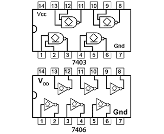
Fig 3.4.6 Open Collector/Drain Buffer ICs
Buffers
Buffers in digital electronics are special gates inserted between one circuit and another to reduce any unwanted interaction between the two. The gates in buffer ICs typically have high impedance inputs and low impedance outputs, giving larger fan out factors than standard gates. Another common use is to enable a logic circuit having a low voltage and/or low current output to drive a circuit or output device requiring higher voltage or current than is available for standard logic ICs.
Open Collector Buffers
Typical ICs using buffered output gates are shown in Fig. 3.4.6. Buffered inverters and non-inverters are common, but there are also gates with other logic functions that have buffered outputs, including some open collector gates, such as the 74HC03 Quad 2 input NAND with open drain from NXP Semiconductors.
Open collector buffers such as the SN74LS06 Hex inverter buffer/driver IC, and the non-inverting buffer SN7407 from Texas Instruments, allow devices such as lamps, motors and relays for example, that normally require higher currents and voltages, to be driven directly from a low voltage logic circuit.
Schmitt Gates

Fig. 3.4.7 Schmitt Gates
The digital signals processed by logic gates need to have fast rising and falling edges. Taking too much time to change logic states, spending too long in the ‘invalid’ zone between states, can cause unreliable logic levels, timing problems and excessive power dissipation, even shortening the life of logic ICs. Standard gate inputs change from 0 to 1 or 1 to 0 at a voltage of about 2.0V. If there is any noise on the input signal, it may be rapidly changing its voltage above and below this level, so causing the gate to rapidly change state if the noise exceeds the noise margin. These rapid and uncertain changes in the gate’s input circuit will also cause the output to oscillate between 1 and 0, transmitting the problem to any subsequent gates in the digital system.
To avoid these problems, gates with Schmitt inputs such as those shown in Fig. 3.4.7 are often used, especially at the input to a system where noise may be expected, as signals arrive from an external source.
Schmitt gates use positive feedback, which causes the gate to switch between logic states extremely quickly. They also have a hysteresis effect, which only allows a change of state to occur as the input voltage passes two specific and different voltages, the Positive-going input threshold voltage (VT+) and the Negative-going input threshold voltage (VT-).
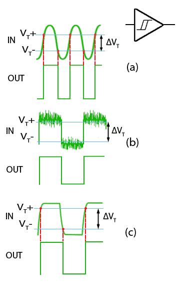
Fig. 3.4.8 Schmitt Gate Action
As the input voltage passes VT+ during a positive going transition, the gate input changes very rapidly to its high state. It then cannot return to its low state until the input voltage falls to the lower level of VT-.
This action has several beneficial effects on poor input signals, as illustrated in Fig. 3.4.8.
(a) It can be used to change slowly changing signals to square waves having very fast transitions.
(b) Noise can be removed from signals, provided that the amplitude of the noise is not greater than ΔVT.
(c) Slow rise and fall times can be restored to practically instant transitions by feeding the signal through a Schmitt trigger.
74 Series Schmitt Gates
Typical Schmitt Hex inverter and Quad NAND gate ICs from the 74 series are illustrated in Fig. 3.4.9.

Fig 3.4.9 Schmitt Input ICs


