
Module 4.1
Binary Arithmetic Circuits
- After studying this section, you should be able to:
- Understand the operation of Binary Adder Circuits.
- • Half Adder.
- • Full Adder.
- • 4 Bit Parallel Adders.
- • 8 Bit Adder/Subtractors.
- • Twos Complement Overflow.
- • Carry Look Ahead Adders.
- Use Free Software to Simulate Logic Circuit operation.
The Half Adder

Fig 4.1.1 The Half Adder
Fig 4.1.1 The Half Adder
Binary arithmetic is carried out by combinational logic circuits, the simplest of which is the half adder, shown in Fig. 4.1.1. This circuit consists, in its most basic form of two gates, an XOR gate that produces a logic 1 output whenever A is 1 and B is 0, or when B is 1 and A is 0. The AND gate produces a logic 1 at the carry output when both A and B are 1. The half adder truth table is shown in Table 4.1.1 and describes the result of binary addition.
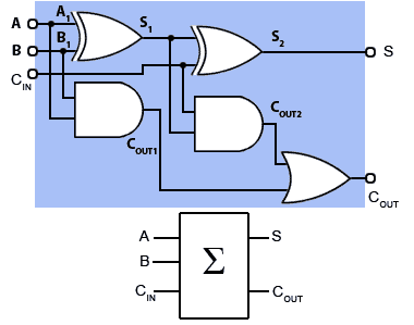
Fig. 4.1.2 The Full Adder Circuit.
1 plus 0 = 12 (110)
and
1 plus 1 = 102 (210)
The half adder is fine for adding two 1-bit numbers together, but for binary numbers containing several bits, a carry may be produced at some time (as a result of adding 1 and 1) that must be added to the next column. As the half adder has only two inputs it cannot add in a carry bit from a previous column, so it is not practical for anything other than 1-bit additions.

The Full Adder
When 2 or more bits are to be added, the circuit used is the Full Adder, shown in Fig 4.1.2, (blue background) together with its simplified block diagram symbol. This circuit simply comprises two half adders, the sum of A and B from the first half adder is used as input A on the second half adder, which now produces a sum of the first half adder sum (S1) plus any ‘carry in’ from the CIN terminal. Any carries produced by the two half adders are then ‘ORed’ together to produce a single COUT. output. The truth table for the circuit is given in Table 4.1.2.

Fig. 4.1.3 4−Bit Parallel Adder.
Parallel Adders
Even the full adder is only adding two single bit binary numbers, but full adders may be combined to form parallel adders, which will add two multi−bit numbers. Parallel adders can be built in several forms to add multi−bit binary numbers, each bit of the parallel adder using a single full adder circuit. As parallel adder circuits would look quite complex if drawn showing all the individual gates, it is common to replace the full adder schematic diagram with a simplified block diagram version.
4 Bit Parallel Adder
Fig 4.1.3 illustrates how a number of full adders can be combined to make a parallel adder, also called a ‘Ripple Carry Adder’ because of the way that any carry appearing at the carry in input (CIN) or produced when adding any of the 4-bit inputs, ‘ripples’ along the adder stages until a final carry out appears at the carry out output (COUT) of the final full adder for bit A3+B3.

Fig. 4.1.4 8−Bit Twos Complement Adder/Subtractor.
8 Bit Twos Complement Adder/Subtractor
To carry out arithmetic however, it is also necessary to be able to subtract. A further development of the parallel adder is shown in Fig.4.1.4. This is an 8-bit parallel adder/subtractor. This circuit adds in the same way as the adder in Fig. 4.1.3 but subtracts using the twos complement method described in Digital Electronics Module 1.5 (Ones and Twos Complement).
When subtraction is required, the control input is set to logic 1, which causes the bit at any particular B input to be complemented by an XOR gate before being fed to input B of the full adder circuit.
Twos complement subtraction in an 8-bit adder/subtractor requires that the 8-bit number at input B is complemented (inverted) and has 1 added to it, before being added to the 8-bit number at input A. The result of this will be an 8-bit number in twos complement format, i.e. with its value represented by the lower 7 bits (bit 0 to bit 6) and the sign represented by the most significant bit (bit 7). The logic 1 on the control input is therefore also fed to the first carry input of the adder to be included in the addition, which for subtraction is therefore:
Input A + Input B + 1
(Here + signifies addition rather than OR)
Alternatively, if addition of A and B is required, then the control input is at logic 0 and number B is fed to the adder without complementing.
Adder/Subtractor Control
")
Fig. 4.1.5 XOR Gate Used as a Data Selector.
How an XOR gate is used here to change the adder into a subtractor by inverting the B inputs can be seen from the truth table for an XOR gate, shown in Table 4.1.3 (in Fig. 4.1.5). Notice that if input A, (used as the CONTROL input) of the XOR gate is at logic 0, then the XOR gate selects input B, but if input A is logic 1, then it selects the inverse of input B (i.e.B).
Twos Complement Overflow
The 8-bit adder/subtractor illustrated in Fig. 4.1.4 is designed to add or subtract 8−bit binary numbers using twos complement notation. In this system the most significant bit (bit 7) is not used as part of the number’s value, it is used to indicate the sign of the number (0 = positive and 1 = negative).
No matter what the word size of a digital system (8-bits 16-bits 32-bits etc.), a given number of bits can only process numbers up to a maximum value that can be held in its designed word length.
During arithmetical operations it is possible that adding two numbers (with either positive or negative values) that are both within the system’s limit, can produce a result that is too large for the system’s word length to hold.
For example, in a twos complement adder such as shown in Fig. 4.1.4, when adding either positive or negative 7-bit values, the result could be larger than 7 bits can accommodate. Therefore the result will need to occupy one extra bit, which means that the calculated value will ‘overflow’ into bit eight, losing a major part (12810) of the value and changing the sign of the result.
To overcome this problem, it is necessary first to detect that an overflow problem has occurred, and then to solve it either by using additional circuits or, in computing, by implementing a corrective routine in software.
Fortunately there is a quite simple method for detecting when an overflow occurs. As shown in Fig. 4.1.5 the overflow detection system consists of a single exclusive or (XOR) gate that takes its inputs from the carry in and carry out connections of the bit 7 (sign bit) adder.
When the carry in (CIN) and carry out (COUT) bits of this adder are examined, it can be seen that if an overflow has occurred CIN and COUT will be different, but if no overflow has occurred they will be identical.
 numbers")
Adding Two Positive (In Range) Numbers
Table 4.1.4 shows the effect of adding two positive values where the sum is within the range that can be held in 7 bits (≤12710). The result of adding two positive numbers has produced a correct positive result with no carry and no overflow.

Twos Complement Subtraction
Table 4.1.5 shows a twos complement subtraction performed by adding a negative number to a positive number. The result is 3110 (within the range 0 to +12710), the sign bit is 0 indicating positive result, CIN and COUT are both 1, so no overflow is detected and the carry bit will be discarded.

Adding Twos Complement Negative Numbers
Table 4.1.6 shows the effect of adding two negative values where the sum is less than +12710 therefore a correct negative result of −7310 (in twos complement notation) has been obtained. Both CIN and COUT are logic 1 and no overflow will be signalled. As only 8−bit calculations are being considered, the carry will be discarded.

Out of Range Result Causes Overflow
When the addition of two positive numbers shown in Table. 4.1.7 results in a sum greater than +12710 the sign bit is changed from 0 to 1, incorrectly signifying a negative result. As the ‘carry in’ from bit 6 to bit 7 is 1 and the ‘carry out’ from bit 7 into the Carry bit is 0 an overflow is detected indicating an incorrect answer.
Notice that if the result of 100111012 were to be considered as an unsigned binary value, the addition in Table 4.1.7 would be correct (15710). However as the calculation is using twos complement notation, the answer of −9910 must be considered as wrong.

Out of Range Addition of Negative Values
Table 4.1.8 shows that adding two negative values can also produce a change in sign and a wrong twos complement result if it is greater than −12810. In this case adding −6310 and −7310 should have produced a negative result of −13610 and not +12010. To check this, the correct answer (although still with the wrong sign) could be obtained if, noting that an overflow had occurred, the answer was complemented and 1 added, giving an unsigned binary result of 100010002 which converts to 128 + 8 = 13610. Overflow errors can be corrected, but this would require either some additional electronics or a software action in response to the overflow signal.
Carry Look Ahead Adders
The adders described in this module are generally called Ripple Carry Adders because of the way that the carry bit is propagated from one stage of the adder to the next, rippling through the chain of full adders until the carry out is produced at the carry out pin of the final stage.
This process takes some time, which is proportional to the number of bits added. Although this may be a minor problem in small adders, with an increase in the number of bits in the binary words to be added, the time delay before the final carry out is produced becomes unacceptable.
To overcome this problem, IC manufacturers offer a range of ‘Carry Look Ahead Adders’ in which the addition and carry out are produced simultaneously. The system uses complex combinational logic to assess whether, at each individual adder a carry will be produced, based on the state of the A and B inputs to that stage, and the logic state of the carry in bit to the first stage.

Fig. 4.1.7 First Stage of a Carry Look Ahead Adder
Fig. 4.1.7 shows an arrangement for producing a carry out by splitting the full adder into a partial full adder (grey block), which has two additional outputs, a propagate (P) output that takes a logic 1 output whenever inputs A and B are 1,0 or 0,1 and a generate (G) output that will be logic 1 whenever the A and B inputs are at 1,1. Using this information it is possible to decide on the logic state of the carry out depending on a combination of the CIN state and the A and B states.
In the carry generator (blue block), the P input is ANDed with the CIN and ORed with the G input to produce a carry out. The carry out is fed to the successive adders in the normal way, but the CIN P and G signals are fed in parallel to the other adder stages, where the state of the carry out for each adder stage can be ascertained from the shared CIN signal and the A and B states for the successive stages, depending on the input states at each stage, rather than waiting for the calculations to complete at all the stages.

Fig. 4.1.8 Carry Look Ahead Adder, Block Diagram
A generalised arrangement in block diagram form (Fig.4.1.8) shows the carry out (COUT) being produced by the parallel carry generator from the A and B input signals and the CIN signal, rather than from the carry out of the final adder stage as in the ripple adders.
The use of look ahead adders is important in practical circuits, not only to speed up operation but because to have an adder that produces part of its answer (the sum) at one time, and another part of its answer (the carry out) at another time, would cause timing problems in other parts of the circuit.

Fig. 4.1.9 M14008B Carry Look Ahead Adder.
A typical example of a Carry Look Ahead Adder is the MC14008B from ON Semiconductor.