Module 4.4
Encoders and Decoders
- After studying this section, you should be able to:
- Recognise the need for Code Converters.
- Understand the operation of Binary Encoders.
- • Priority Encoders.
- • Diode Matrix Encoders.
- Understand the operation of Decoders/Demultiplexers.
- • Basic decoder operation.
- • 74 series Decoder ICs.
- • BCD-to-Decimal.
- • BCD to 7 Segment.
- • Address Decoders.
- Understand common features on Decoders/Demultiplexers.
- • Chip Enable.
- • Decoder display options.
- • Cascaded Decoders.
- • Display blanking.
- • Ripple blanking.
- • Latching Decoders.
- Simulate circuit operation using software.
Binary Encoders
Digital Electronics Module 1 (Number Systems) described a number of different binary codes that are used to perform a range of functions in digital circuits. Mathematics, graphics, data manipulation and physical control systems are among many of the functions that are carried out using binary data, and each of these uses may require binary data arranged in various forms of binary codes. For example text may be represented by an ASCII code (American standard Code for Information Interchange), in which each letter, number or symbol is represented by a 7-bit binary code. Decimal numbers in a calculator may be sent to a numeric display using BCD (Binary Coded Decimal). Notice that the word ‘code’ appears in each of these titles, and a binary code differs from normal binary because it is arranged in a particular way to suit a given purpose.
Priority Encoders
Binary Encoders generally have a number of inputs that must be mutually exclusive, i.e. only one of the inputs can be active at any one time. The encoder then produces a binary code on the output pins, which changes in response to the input that has been activated.
Priority Encoding
Because it is always possible when using input switches that more than one input may be active at a single time, most encoders of this type feature ‘priority encoding’ where, if more than one input is made active at the same time, the output will select only the most significant active input. For example, if 6 and 7 are pressed together the BCD output will indicate 7. The Pinout diagram for the 74HC147 10-to-4-line priority encoder from NXP (Philips Semiconductor), is illustrated in Fig.4.4.1.
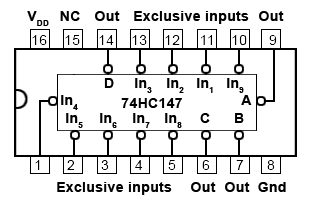
Fig. 4.4.1 74HC147 10-to-4-Line Priority Encoder
Depending on the encoding purpose, each each different IC has its own particular method for solving encoding problems. For example, a simple decimal to BCD (or 10-to-4 line) encoder would be expected to have ten input pins, but in fact the 74HC147 has only 9. The tenth condition (zero) is assumed to be present because when none of the 1 to 9 input pins is active, this must indicate zero.
The input pins may be used to connect to switches on a decimal keypad, and the encoder would output a 4-bit BCD code, (00002 to 10012) depending on which key has been pressed, or simply to identify which one of ten input lines in a circuit is active, by outputting an appropriate number in four bit BCD code.
Chip Enable Inputs
Some other encoder ICs also feature extra inputs and outputs that allow several ICs to be connected together to achieve more flexibility in the numbers of input and output lines available. These include ENABLE inputs, (typically labelled E), which may consist of one or more input pins that need to have a particular logic level applied (usually logic 0) in order to activate the encoding action. In the absence of a correct ENABLE signal the output pins of the IC will remain in their inactive state.
Switch Bounce
One problem with combinational logic circuits is that unintended changes in output data can occur during the times when the outputs of the IC are changing. This can be due to problems such as switch contacts ‘bouncing’ as they close, creating rapid and unpredictable changes in logic levels for a very short time, however logic IC operate at high speed and will respond to these very fast changes.
Race Hazards
Problems can also occur due to ‘race hazards’ where different paths that digital signals take through a logic circuit may have different numbers of gates. For example two logic signals that change simultaneously at two circuit inputs may take different routes through the circuit before being applied to some common gate later in the circuit. However, if one signal passes through six gates for example, while the other signal passes through seven gates, each of the signals will have encountered a different total propagation delay due to the different number of gates they encountered. Therefore they will each arrive at the common gate at slightly different times, and so for a very short time an unexpected logic level may occur at that gate output.
In using combinational logic ICs such as an encoder, problems like switch bounce and race hazards must be allowed for, and one (though not necessarily the best) solution can be to temporarily make the ENABLE pin high during times when data is likely to change. This disables the encoder for a short time until the signal data has settled at its new state, so that there is no chance of errors at the output during changes of input signals.
74HC148 8-to-3-Line Encoder
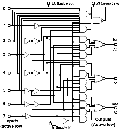
The 74HC148 also uses priority encoding and features eight active low inputs and a three-bit active low binary (Octal) output. The internal logic of the 74HC148 is shown in Fig. 4.4.2
The IC is enabled by an active low Enable Input (EI), and an active low Enable output (EO) is provided so that several ICs can be connected in cascade, allowing the encoding of more inputs, for example a 16-to-6-line encoder using two 8-to-3 encoders. The CMOS 74HC148 also uses active low inputs and outputs. The operation of the 74HC148 can be seen from its truth table shown in Table 4.4.1.
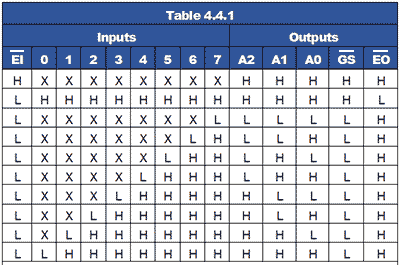
Notice from Table 4.4.1 that the IC is only active when EI is low, and also that for each input selected by a low logic level (L), all lower value inputs indicate ‘Don’t Care’, typical of priority encoding.
Two further outputs (GS and EO) are used for connecting additional 74HC148 ICs in cascade.
The EI input is normally used on the most significant IC and whenever an input on this IC is selected, the EO output goes high (disabling any less significant ICs), and the Group Select (GS) output goes low indicating that the group of outputs of this IC are active.
16-to-4-Line Encoder
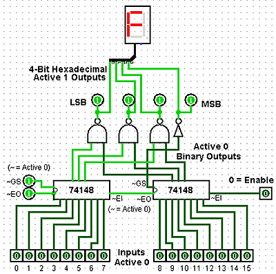
Fig 4.4.3 shows a simulation created in Logisim, which demonstrates how two 74HC148 ICs can be connected in cascade to make a 16-to-4-line encoder. Notice how EI is used to enable the most significant encoder, and how EO and EI in the centre of the diagram are used to cascade the ICs. As the output (000016 to FFFF16) will now require 4 bits. The GS (Group Select) pin, which changes to its low logic state when any input on the most significant IC is active, is used to create the fourth output bit, (23) for any output value above 7.
In this simulation, available from Module 4.6, the active low outputs of the encoder have been inverted to provide active high inputs to the hexadecimal display.
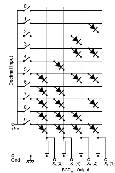
Fig. 4.4.4 Diode Matrix Decimal-to-2421 BCD Encoder
Diode Matrix Encoders
Where encoders are needed for non-standard applications, they can also be implemented using a diode matrix, such as the decimal-to-BCD2421 encoder shown in Fig 4.4.4.
In this example, as any one of the ten switches is closed +5V is applied to just one of the horizontal lines. Any diode that has its anode connected to that horizontal line and its cathode connected to a vertical line (that is held at zero volts by a resistor connected to Gnd) will conduct.
When current flows through any of the resistors, the top of that resistor will be at +4.4V (i.e. +5V minus a 0.6V drop in across the diode), which will be seen by the output as logic 1.
For example if switch 6 is closed, the two diodes connected between line 6 and columns X3 and X2 will conduct, making outputs X3 and X2 logic 1 and giving a binary2421 output word of 11002 (or 2+4 =610).
This particular diode matrix will therefore give an output in BCD2421 code from 00002421 to 11112421 for closure of switches 0 to 9.
Many other output sequences are possible therefore, by using different arrangements of the diode positions.
Although the encoder circuits described in this module may be used in a number of useful encoding situations, they have some features that limit their use for realistic keyboard encoding.
• Priority encoders do not sense information from two or more keys that are pressed at the same time.
• Switches on keypads normally contact for only a brief time, these basic encoders are not able to store and remember the data input from a pressed key once it is released.
• When a switch is closed the contacts may ‘bounce’ giving several brief 1 and 0 logic states, when ideally there should be only one change in state for each key press.
To overcome common problems such as these, a more complex circuit (or IC) is required. These will typically have features such as key bounce elimination, built in data memory, timing control using a clock (oscillator) circuit and some ability to differentiate between two or more keys pressed at the same time. Another important feature is the ability to signal to the system that the keyboard is controlling, when a key has been pressed and new data needs to be read.
For small keypads having less than 20 keys the processing has typically been carried out by an ASIC (Application Specific Integrated Circuit) such as the MM74C922 Keyboard Encoder although this IC is now being listed as obsolete by some manufacturers, as many modern circuits, especially those with more keys, use a dedicated microprocessor or micro-controller (MCU) to carry out keyboard decoding.
Binary Decoders
These circuits in IC form are often called Decoders/Demultiplexers and perform the opposite function to an encoder (or multiplexer).
Binary data is used in digital circuits in the form of one or another binary code, which is an arrangement of the binary bits in a particular order to represent ‘real’ quantities such as a set of decimal numbers (BCD code) or text (ASCII). In a complete digital system therefore it is often necessary to convert one code to another, or to convert a binary code to drive some user interface such as a LED display.
A decoder is a combinational logic circuit that takes a binary input, usually in a coded form, and produces a one-bit output, on each of a number of output lines. The logic state (1 or 0) on any of the output lines depends on a particular code appearing on the input lines.
2-to-4-Line Decoder
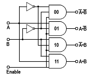
For example, a 2-to-4-line decoder is shown in Fig. 4.4.5, in this circuit the two input lines can be set to any one of four binary values, 00, 01, 10 or 11. Resulting from this input, and provided that the (active high) Enable input is set to logic 1, the output line corresponding to the binary value at inputs A and B changes to logic 1. The other output lines remain at logic 0.
When the binary value at inputs A and B changes, the logic 1 on the output changes to a different line as appropriate. If the enable input is set to logic 0, all the outputs remain at logic 0 whatever values appear at inputs A and B.
To obtain a logic 1 at any of the four outputs, the appropriate 3 input AND gate must have all of its inputs at logic 1. Provided that the Enable input is at logic 1, the output is controlled by using NOT gates to invert the logic applied from inputs A and B as required.
For example if inputs A and B are both at logic 0, the NOT gates at the inputs to the top (00) AND gate, invert both 0 inputs to logic 1, and therefore logic 1 appears at the 00 output. The 01 and 10 AND gates each have one input directly connected to the A or B input, whilst the other input is inverted.
The 11 gate has both A and B inputs directly connected to the AND gate so that 112 applied to A and B results in logic 1 at the 11 output.
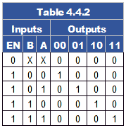
Fig. 4.4.5 Two-to-Four-Line Decoder
Notice the similarity between Fig 4.4.5 and the 4-to-1-Line Multiplexer shown in Fig 4.2.4. In fact Fig. 4.4.5 could act as a demultiplexer for Fig 4.2.4 if the A and B inputs are used as control lines, and the enable input of Fig 4.4.5 used as the single data input. This example of dual use explains why decoders are often called Decoder/Demultiplexers. The circuit operation of Fig. 4.4.5 is shown in truth table form in Table 4.4.2, and a Logisim Simulation of Fig. 4.2.4 and Fig. 4.4.5 working together as a Multiplexer/Demultiplexer pair can be downloded from our Logisim page.
74 Series Decoder ICs
2-to-4-line decoders (also called 1 of 4 decoders) are commercially available in both HC and HCT types in a number of versions from different manufacturers. These are typically dual packages such as the 74HC139 from NXP with two decoders per chip. One difference, (commonly used) from the basic example shown in Fig. 4.4.5 is that the outputs, and sometimes also the inputs, on such ICs may be ‘active low’ meaning that the active or logic 1 state is at the lower voltage of the two possible logic states, so that the output is sinking current when it is ‘logic 1’. This provides a greater drive capability than would be available if logic 1 was at its high voltage, and sourcing current.
Also, decoder ICs are very often used to activate the Enable or Chip Select (CS) inputs of other ICs, which are usually active low, so having a decoder with an active low output saves using extra inverter gates.
Another feature found in 74 series ICs is the common presence of buffer gates (which may be inverting or non-inverting) at the IC inputs and outputs to give improved input and output capabilities Clamp diodes and current limiting resistors are also often incuded at the inputs and outputs to give improved protection from high electrostatic external voltages.
BCD-to-Decimal Decoder
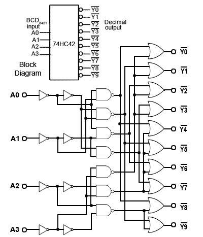
The 74HC42 BCD-to-Decimal decoder IC from Texas Instruments contains a more complex circuit, as illustrated in both block and logic schematic form in Fig. 4.4.6.
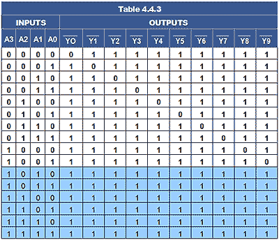
The input is in 4-bit BCD8421 format, and each of the ten outputs, labelled Y0 to Y9 produce a logic 0 for an appropriate BCD8421 input of 00008421 to 01018421. Any input value greater than 01018421 results in all of the output pins remaining at their high level, as shown in pale blue in Table 4.4.3.
Note that the truth table (Table 4.4.3) shows the appropriate high and low logic levels as 1 and 0 respectively to match the logic levels shown in the downloadable Logisim simulation.
On most data sheets for ICs the levels are shown as H (the higher voltage) and L (the lower voltage) to avoid confusion in cases where negative logic is used.

Fig 4.4.7 Cold Cathode Display
BCD to decimal decoders were originally used for driving cold cathode numerical displays (Nixie tubes), which are neon filled glass plug-in tubes with ten anodes in the shape of numbers 0 to 9 that glow when activated by a high voltage.
However, decimal decoders are also useful for a variety of other uses. Remember that decoders are often also called demultiplexers, as they can be used for many demultiplexing tasks and for driving devices such as lamps, motors and relays in control systems.
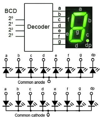
Fig. 4.4.8 Driving a 7 Segment Display
BCD to 7 Segment Decoders
Because cold cathode displays require a high voltage drive, they have mostly been replaced by low voltage LED or LCD displays using 7 segment displays, therefore the BCD-to-7-segment decoder has become one of the most commonly available decoders.
As shown in block diagram format in Fig. 4.4.8, this type of decoder has 4 inputs for binary coded decimal and an output for each of the 7 LEDs that make up the 7-segment display. The eighth LED (labelled dp or sometimes h) will normally be controlled by some extra logic outside the decoder. 7-segment displays may have a common cathode connection, needing to be driven by logic 1 outputs, or common anode connection requiring logic 0 outputs from the decoder.
Decoder/Drivers
Depending on the decoder IC and display type used, although it may sometimes be necessary to use a transitor amplifier to drive each segment of the display, there are Decoder/Driver ICs available, such as the 74LS46, 47, 48 and 49 that have sufficient output current and a choice of output designs such as open collector, internal pullup resistors and active high or active low output levels that allow direct connection to both led and filament lamp displays.
7-Segment Fonts

Fig. 4.4.9 Typical 7 Segment Font
When illuminated by the correct logic levels, the seven-segment display will show all the decimal numbers from 0 to 9. Depending on the logic design of the IC, some decoders will automatically blank the display for any value greater than 9, while others display a unique (non-numeric) pattern for each value from 10 to 15 as shown in Fig. 4.4.9, and may display 6 and 9 with or without a ‘tail’. For displaying Hexadecimal numbers, the letters A b C d E and F are used to avoid confusion between capital B and 8, and capital D and 0.
74LS49 BCD to 7-Segment Decoder
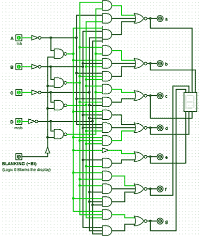
Fig. 4.4.10 is a screen grab from Logisim, showing a working simulation of a basic BCD to 7-segment decoder (based on the 74LS49 in the TTL range of 7-segment decoders from Texas Instruments). This IC uses the font illustrated in Fig. 4.4.9 and a single active low BI pin for use as a blanking input.
Blanking
The blanking input pin BI can be used to turn off the display to reduce power consumption, or it can be driven with a variable width pulse waveform to rapidly switch the display on and off thereby varying the apparent brightness of the display.
Making the BI input logic 0 blanks the display whatever data is present at the decoder BCD inputs.
74LS48 BCD to 7-Segment Decoder Features
Ripple Blanking
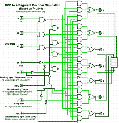
As a BCD to 7 Segment decoder is designed to drive a single 7 segment display, each digit of a numeric display is driven by a separate decoder, so where multiple digits are required, a technique called Ripple Blanking is used, this allows the blanking inputs of several ICs to be connected in cascade. The Ripple Blanking Output (RBO) of the first decoder IC (controlling the most significant digit) is fed to the blanking input pin of the next most significant digit decoder and so on.
When Logic 0 is applied to the ripple blanking input (RBI) of a decoder, it blanks the display only when the BCD input to that particular decoder is 0000. A logic 0 input will therefore blank any display digit that is 0. This allows for the suppression of any leading or trailing zeros in numbers such as 00000077 or 7.7000000.
There are a number of BCD-to-7-segment decoder ICs in the 74 series (types 7446 to 7449) each with different variations, such as active high or active low outputs, high current driver outputs, a choice of display font (whether the 6 and the 9 have a ‘tail’ or not), and a lamp test input to check that all LEDs are working.
Fig. 4.4.11 is a screen grab of a BCD to 7-segment decoder using these advanced features. Click the ‘Simulation Available’ button to download a working simulation for this circuit. Note that although the simulation works in a similar manner to a real decoder such as the 74LS48, because the BI input and RBO output on the real chip share a common pin, this creates problems for the simulator. Therefore the logic has been changed by using two tri-state buffers to separate the input and output signals.
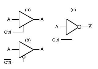
Fig. 4.4.12 Tri-State Buffers
Tri-State Logic
The simulation illustrated in Fig. 4.4.11 uses two tri-state buffers(also called 3-state buffers) to achieve isolation between a shared input and output pin. The necessary isolation was achieved by using two simple tri-state buffers, shown in Fig 4.4.12 so that the shared pin can be an input or an output, but not at the same time.
The tri-state buffer (a) in Fig. 4.4.12 has an input and an output just like a normal buffer, but it also has a control (Ctrl) input. This input, when held at logic 1 enables the buffer, so whatever logic level appears at its input also appears at its output.
When logic 0 is applied to the Ctrl input however, the buffer is disabled and its output assumes a high impedance state. That is, it will take up whatever logic level occurs on the line connected to its output, no matter what logic level is on its input. It is effectively open circuit, just as though making the enable input low had opened a switch between its input and output.
Tri-state buffers are also available with an active low Ctrl input, that are enabled by logic 0 (b), and as inverting buffers, that invert the output when Ctrl is activated (c).
There are whole ranges of devices that have 3-state outputs. Devices such as microprocessors and memory chips, intended for use in bus systems, where many inputs and outputs share a common connection (e.g. a data bus) normally have tri-state outputs. However, apart from very large scale integrated (VLSI) devices, such as computer ICs, 3-state logic is not generally used within MSI ICs as shown in Fig 4.4.11. In these smaller scale ICs, alternatives such as open collector logic are more suitable. Discrete 3-state logic components are more often used for connections between, rather than within ICs.
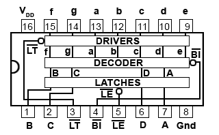
Fig. 4.4.13 The 74HC4511 Latching BCD-to-7-Segment Decoder
Latching BCD-to-7-Segment Decoders
In common with modern practice, TTL ICs are not generally recommended for new designs and are superseded by newer HC and HCT versions. Apart from the advantage of lower power on these versions, a common feature added to these ICs is a ‘Data Latch’. This is a one nibble memory (for the 4 bit BCD input) controlled by a Latch Enable (LE) pin, which allows the decoder to store the 4 bit input present, when LE is logic 0 so that only the stored data is displayed. When the latch is not enabled however, it becomes ‘transparent’ i.e. any changes in the data appearing at the inputs are fed directly to the display. It is also common on later ranges of decoders that any input values greater than 1001BCD (910) are automatically blanked. Fig. 4.4.13 shows a typical pin-out for a CMOS BCD-to-7-segment decoder. Examples of these ICs are the MC14513 from ON Semiconductor and the 74HC4511 from NXP (Philips Semiconductors).
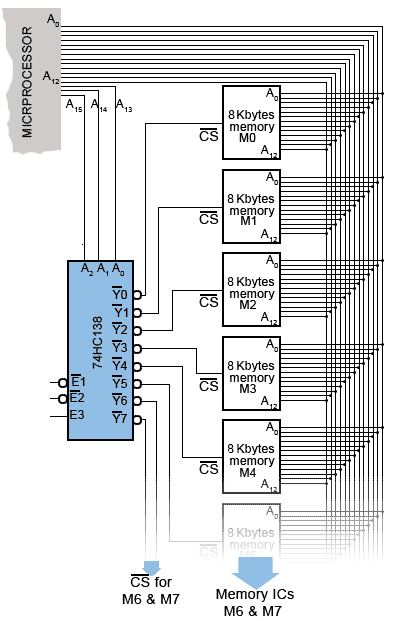
Fig. 4.4.14 Address Decoding
Address Decoders
Decoders may also be used in computer systems for address decoding. Fig. 4.4.14 illustrates a typical application where a 74HC138 3-to-8-line decoder is used to enable the microprocessor to communicate with many locations in its memory system. The memory in this example comprises 8 x 8Kbyte memory ICs, therefore each IC contains 8192 x 1 byte locations giving a total number of 8 x 8192 = 65536 locations, each having a hexadecimal location number (an address) from 000016 to FFFF16.
To contact any of these memory locations, the microprocessor outputs the address of the required memory location on the 16-bit address bus, which can hold any one of 216 = 65536 different values. However, the memory in this example is made up from 8 identical ICs, each holding 8192 locations, and as this number of locations can be addressed by 213 = 13 address lines, lines (A0 to A12) are connected from the microprocessor to the 13 address inputs of each memory IC. This common connection means that each of the memory chips will have the same address range as all the other memory ICs, and therefore any address within the range 000016 to 200016 (819210) put out by the microprocessor will contact the same address in all 8 memory ICs. This obviously creates a problem; each memory chip should have its own range of addresses with the 8 ICs forming a continuous address sequence in blocks of 819210 locations.
This is where the address decoder is used. Notice that, in Fig. 4.4.14 the three highest order address lines (A13, A14 and A15) are connected to the 3 address inputs (A0, A1 and A2) of the 74HC138 3-to-8-line decoder. Therefore, provided that the three Enable inputs (E1,E2and E3) of the decoder are fed with the appropriate logic levels to enable the decoder, each of the Y0 to Y7 pins of the decoder will output a logic 0 for one of the 8 possible combinations of the three bit value on the address lines A13 to A15.Since this three bit value will only change when the 16-bit value on the address bus changes by 819210 (200016) the memory chips will be selected using their chip select (CS) inputs, every 8 Kbytes. The eight memory ICs will therefore provide a sequential set of memory locations covering the whole 64K of memory, addressable by the microprocessor.
The 74HC138 Decoder
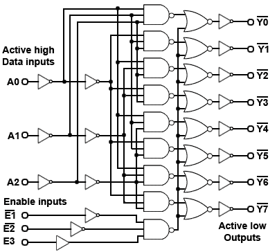
The combinational logic of a typical 3-to-8-line decoder based on the 74HC138, is illustrated in Fig. 4.4.15, an IC that has many uses apart from address decoding, it is often used with a binary counter driving its inputs, when its eight outputs constantly step through a 0 to 7 sequence. Typical applications include sequence generating for lamp control, row scanning for dot matrix displays, digital operation of analogue controls and anywhere that a sequence of unique outputs is required.
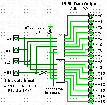
Data sheets for the 74HC138 point out the advantages of the three Enable pins, which can be used for simply connecting the decoders together to make larger decoders. An example of this is shown in the downloadable Logisim simulation Fig. 4.4.16, where two 74HC138 ICs are connected together using only one additional NOT gate.
Note that the pin connections on the ICs in Fig. 4.4.16 are not in the consecutive 1 to 16 order of the real 74HC138 pinout, but can be identified in the downloaded simulation by hovering your mouse over any pin.
The E1 (active LOW) input is used here as the fourth (23) data input so that for a count of 0 to 710 (00002 to 01112) at the inputs, the logic 0 applied to E1 enables the top IC and disables the bottom IC via the NOT gate, but for a count between 10002 and 11112 )810 to 1510)the fourth data input (E1) becomes logic 1 and the situation is reversed, with the (active low) output continuing its (810 to 1510) sequence on the bottom IC.


