Module 1.2
Class A Biasing
- After studying this section, you should be able to describe:
- The Reasons for DC Bias in Amplifiers.
- Advantages and Disadvantages Class A Bias.
- Simple Common Emitter Fixed DC Bias.
- • The Use of Input Characteristics.
- • Quiescent Conditions.
- • Preventing Distortion with Correct Bias.
- • Output Characteristics.
- • Load Line.
- • Basic Fixed Bias Calculations.
- Bias Stabilisation.
- • Collector Derived Bias.
- • Base Bias networks.
- • Emitter Stabilisation.
- • Use of Emitter Bypass Capacitors.
- FET Biasing.
An Amplifier´s Common Connection
Transistors in amplifiers commonly use one of three basic modes of connection. A transistor has three connections (collector, base and emitter), whilst the input and output of an amplifier circuit each require two connections, making four in total, therefore one of the transistor´s three connections must be common to both input and output. Whether collector, base or emitter is chosen as being common to both input and output has a marked effect on how a transistor amplifier operates. This section describes how the transistor is biased in common emitter mode, the most commonly used of the three connection modes for voltage amplifiers.
Class A Bias
Class A amplifiers are biased with a DC voltage applied across the transistor base-emitter junction so that their quiescent (or no signal) operating point is on a linear part of the transistor’s characteristics. Also, the signal waveform applied to the base should not drive the transistor either into saturation or into cut-off. If this were allowed to happen it would cause the waveform peaks to be flattened, causing distortion. In class A biasing, the collector voltage is kept at approximately half the supply voltage, however this means that the transistor is permanently passing collector current, even when no signal is applied, so power is being wasted, and although class A provides for very low distortion, it is also relatively inefficient in its use of power.
The theoretical maximum efficiency of a class A amplifier is 50% but in practice the figure would be nearer 25%. The main use for class A bias is in low power audio and radio frequency voltage amplifiers, where the amount of power wasted is less significant than the amplifier´s main advantage of low distortion. However class A may also be used for low distortion power amplifiers in mains (line) powered hi-fi audio systems where efficiency is less vital.
Common Emitter Fixed Biasing
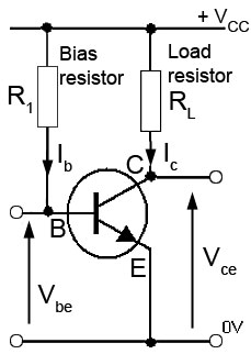
Fig 1.2.1 Simple common emitter bias.
Amplifiers are needed in most pieces of electronic equipment, not only for sound and picture reproduction but also in control systems and communications. The design of amplifiers is aimed at producing a circuit that has a predicted gain over a particular band of frequencies with minimum distortion. The amplifier must also be stable and not prone to oscillation. Bipolar PNP or NPN transistors or FETs may be used in a wide variety of designs depending on their intended purpose.
Consider the simple bipolar NPN common emitter amplifier shown in Fig. 1.2.1 consisting of a transistor and two resistors. To function correctly the amplifier should produce at its output, an amplified version of the signal at its input without distortion. In order to do this, its quiescent or no signal (DC) conditions, must first be correct. Its output can only be undistorted if its input is undistorted.
Using the Input Characteristics.
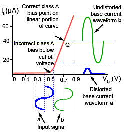
Fig. 1.2.2 Input Characteristics.
Fig. 1.2.2 shows a typical input characteristic curve for a small signal amplifier transistor where changes in base voltage Vb are plotted against the resulting changes in base current Ib.
If changes in the AC signal voltage (changes in Vb) applied to the base, are to produce proportional changes in AC base current Ib then some DC value of VB must be used so that positive and negative excursions of the signal voltage occur only on the linear part of the input curve (waveform b in Fig. 1.2.2). This DC voltage (0.7V in Fig. 1.2.2) applied to the base is called the base bias voltage. It can be seen from Fig. 1.2.2 that if the bias voltage is insufficient, then only the positive tips of the input voltage waveform would produce base current, and consequently severe distortion will occur in the base current waveform a.
It can also be seen that for this transistor, a DC base bias voltage (RB) of 0.7V produces a quiescent (DC) base current of 40µA. These values are set by the correct choice of resistance value for RB (Fig. 1.2.1).
Setting the Quiescent Output Conditions
The quiescent output conditions must also be considered, as the quiescent base current Ib will produce a quiescent collector current Ic that will depend on the value of Ib and the current gain hfe of the transistor. Also, because Ic flows through the load resistor (RL) it will produce a potential difference across RL that when subtracted from the supply voltage (Vcc) gives the value of the transistor collector/emitter voltage (Vce).

Fig. 1.2.3 Incorrect Bias Conditions.
Fig. 1.2.3 shows the two extreme conditions for the values of Ic and Vce. It can be seen in the first case (Fig. 1.2.3a), that if the collector current IC is zero, owing to the base voltage being low enough to cut off base current, the voltage developed across RL will be zero and the whole of Vcc will be developed across the transistor so Vce will rise to the supply voltage Vcc.
If a signal is applied under these conditions (Fig. 1.2.3a), positive going half cycles of the output signal (which is in anti phase to the voltage waveform at the base) cannot make Vce rise any further than Vcc and so the positive going half cycles of collector voltage will not be reproduced, causing severe distortion.
Alternatively if Ic is very high (Fig 1.2.3b) due to excessive base bias, the transistor will be in a saturated condition and Vce will fall to almost zero. As the collector voltage cannot fall below 0V the negative going half cycles of the output signal will be lost. It follows therefore, that to reproduce the full waveform at the collector, the ideal quiescent value for Vce will be around midway between Vcc and zero volts. This will allow the maximum amplitudes of both positive and negative going half cycles of the output wave to be reproduced without distortion.
Using the Output Characteristics
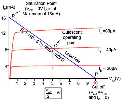
Fig. 1.2.4 Output Characteristics and Load Line.
In the output characteristics shown in Fig. 1.2.4 changes in Ic are plotted against changes in Vce for various constant base currents Ib .
A ´load line´ is drawn on Fig. 1.2.4 between the two extreme points described in Fig. 1.2.3.
Point P is where VCE = Vcc (which in this case equals 10V) and Ic= zero, and because no current collector is flowing, the transistor is said to be "Cut off".
Point R is the maximum value of Ic (where Ic = Vcc ÷ RL) and Vce is zero (because practically the whole of Vcc is developed across RL). This is called "Saturation" as no further increase in collector current will occur.
With the load line drawn from P to R, it can be seen that a value of Vce can be chosen mid-way along the load line at point Q, which in this case coincides with the curve for IB.
A vertical line projected downwards from Q then intersects the VCE axis midway between Vcc and zero, and a horizontal line projected from Q intersects the IC axis to give a quiescent value of 8mA.
From the values of VCce and IC indicated, it is now possible to calculate a value for RL using:
RL = (Vcc - Vce ) ÷ Ic
So using the load line at point Q (or any other point with different pairs of values):
RL = (10 − 5) ÷ 8 x10−3 = 625Ω
Biasing an amplifier so that the operating point is at the center of the linear part of the transistor´s characteristic curves is called ´Class A bias´.
Example:
Design the DC fixed bias conditions for the simple class A common emitter amplifier shown in Fig. 1.2.1, assuming a supply voltage (Vcc ) of 10V using a transistor with a common emitter current gain (hfe) of 200.
From the input characteristics (Fig. 1.2.3) Ib needs to be 40µA which indicates a value for Vbe of 0.7V.
Therefore:
Rb = ( Vcc - Vbe) ÷ Ib
= (10 − 0.7) ÷ 40µA = 232.5KΩ
Because, in a practical circuit, the nearest preferred value for the base resistor Rbwould be chosen to make Rb = 220KΩ.
Since the base current chosen is 40µA and the transistor hfe is 200:
IC= Ib x hfe = 40µA x 200 = 8mA
If a collector current (Ic) of 8mA is sufficient to drop Vce to 5V (half of Vcc) then 16mA will cause Vce to fall to practically zero and saturate the transistor. 16mA will therefore be point R on the load line.
As the quiescent collector voltage is to be 5V (half of Vcc), and the voltage across RL is also 5V, it is possible to calculate the value of RL to give the correct conditions at point Q:
RL = VRL ÷ Ic = 5V ÷ 8mA = 625Ω
or approximately 680Ω (the next higher resistor preferred value).
Problems with the fixed bias design.
While the design described in Fig. 1.2.1 is simple and requires a minimum of components, there are some problems that need to be overcome for practical use.
If, the supply voltage or transistor temperature changes for any reason, the bias voltage will also change. If the bias voltage increases then more base current will flow, which will cause an increase collector current. This will in turn cause a rise in junction temperature within the transistor, and so, a further increase in current. The transistor will then pass even more current, creating a further rise in temperature and so on.
The ultimate result of this process called "Thermal Runaway", is that the transistor will get hotter and hotter until it is destroyed. Although Thermal Runaway is much less of a problem in modern power transistors, in small signal types it is still a possible hazard that should be avoided by building some form of bias stabilisation into the amplifier design.
DC Stabilisation
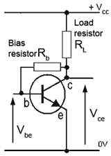
Fig. 1.2.5 Collector Derived Bias.
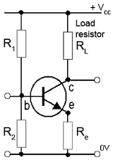
Fig. 1.2.6 Emitter Stabilisation
Fig. 1.2.5 shows a simple method of improving the temperature stabilisation of a common emitter amplifier. Instead of feeding the bias current from Vcc it is fed from the collector end of RL.
With this arrangement, any increase in collector current will cause an increase in the potential difference across RL and, as the top of RL is held steady by Vcc, the collector voltage Vce at the bottom of RL must fall. This in turn will cause Vbe to fall, and so reduce collector current. The bias conditions are to a large extent self adjusting and said to be stabilised by a form of DC feedback.
Emitter Stabilised Bias
An alternative, and much more common bias arrangement used in most commercial circuits, uses a potential divider comprising two resistors (R1 and R2 in Fig. 1.2.6) to provide a steady value of Vbe and an emitter resistor Re to provide stabilisation by DC feedback.
If collector current increases in this circuit, so does the emitter current, which causes a rise in the emitter voltage Ve. This rise compared with the steady base voltage, causes a reduction in the base-emitter voltage Vbe and subsequent drop in collector current. DC feedback using an emitter stabilising resistor keeps circuit conditions stable when other conditions (e.g. temperature or transistor hfe) may change.
However the emitter resistor will also cause unwanted AC feedback because under signal conditions the AC waveform appearing on the emitter will be in phase with the base waveform, and the two waveforms changing together will tend to reduce the variations in base-emitter voltage, causing a substantial reduction in gain. To avoid this problem it is usual for the emitter stabilising resistor Re to be bypassed by a (usually) large value capacitor connected across RE that will form a very low impedance path to any AC signal present, preventing any AC appearing on the emitter, but without changing any of the DC conditions.
FET Biasing
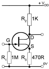
Fig. 1.2.7 FET Bias.
The biasing of FETs is simpler than in bipolar designs as no gate (input) current is flowing. Fig. 1.2.7 shows a typical JFET bias arrangement. (MOSFETs also use a similar bias circuit).
When used in depletion mode, the gate of the FET must be more negative than the source. This is achieved by holding the gate at zero volts, whilst the drain/source current through R3 makes the source terminal positive. As no gate current flows in FETs there can be no voltage developed across R1 and the gate remains at zero volts. The use of a very high value for R1 maintains the very high input impedance, which is a useful property of FET amplifiers.
An AC signal applied to the gate will cause small variations of gate voltage above and below zero, which will cause AC changes in drain-source current and, as in a bipolar amplifier, these are converted to voltage changes by R2. The source resistor R3 performs DC stabilisation in the same way as the emitter resistor in a bipolar amplifier, and is also normally bypassed to prevent AC negative feedback.
Top of Page


