Google Ads
Module 2.1
Class A Amplifier Design
- After studying this section, you should be able to:
- Design a basic class a Common emitter audio amplifier.
- • Understand appropriate design and component requirements for a class A amplifier.
- • Calculate resistance values for DC bias conditions.
- • Assemble a prototype amplifier on Breadboard.
- • Use a multimeter to carry out appropriate tests to confirm operation.

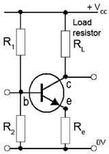
Fig. 2.1.1 Amplifier DC components
Part 1. Designing the DC Conditions.
As you work through the design process, record your results of your calculations and design decisions on the Amplifier Design Record sheets, you will need these results when building the amplifier.
Calculate the component values and record your results in Part 1 of the Amplifier Design Record sheets.
1. Decide on the DC supply voltage VCC
This should be less than the maximum VCEO voltage for the transistor you intend to use and will also depend on the available supply; this may be a bench power supply or a battery. Values of 6 to 12 volts are common for a common emitter voltage amplifier.
2. Choose a transistor
The prototype amplifier for this exercise used a NPN small signal transistor such as the 2N3904, but other similar transistors should work equally well. A datasheet for the 2N3904 can be downloaded from www.datasheetcatalog.com or you could choose a different general purpose NPN small signal transistor and download its datasheet.
3. Decide on a suitable quiescent collector current Iq
Iq is the Collector current when no signal is applied. The maximum value must be less than the maximum IC(max) figure for the transistor. However using a high value of current will waste power as the circuit is supposed to be a VOLTAGE amplifier so current should be kept quite low, but the lower the current you choose, the higher the value of RL will be. This increases the output impedance of the amplifier (which will be approximately the value of the load resistor) and ideally this should be low. A compromise figure of 10 to 20% of the transistor´s IC(max) figure shown on the data sheet should be OK for a maximum value of Iq but a commonly selected current of around 1mA would be typical for a small general purpose amplifier transistor.
4. Calculating a value for the load resistor RL
Once the supply voltage and collector current are decided, the value of the collector resistor can be calculated. The transistor quiescent collector voltage needs to be about half of VCC so that the output signal can swing by equal amounts above and below this value without driving the transistor into saturation (0V and maximum collector current) or cut off (zero current and VC equal to the supply voltage). RL will therefore be half of VCC divided by Iq.
Note that whenever a component value has been calculated, it is unlikely that the result of the calculation will match any of the available preferred values of real resistors. Therefore you will need to choose the nearest preferred value.
5. Calculating the value of RE
To provide efficient bias stabilisation, the emitter voltage VE should be about 10% to 15% of VCC. So choosing a value of 12% of VCC for VE and assuming that IE is the same as IC (It is only different by the small amount of the base current), a value for the resistor RE can be calculated by dividing the emitter voltage VE by the emitter current IE then choosing the nearest preferred value.
6. Estimate a value for base current IB
This can be found by dividing the collector current IC by the transistor´s current gain hfe obtained from the data sheet. Because the hfe varies from one transistor to another, even of the same type, it may be quoted as a typical value or as a range between minimum and maximum values, hfe also varies with collector current so whatever figure you choose for hfe, the result of calculating IB will be an approximation so the base voltage will probably not be accurate. However this can be ‘fine tuned’ when the amplifier is being constructed.
7. Calculating VB
The base voltage should be about 0.7V (700mV) higher than VE to ensure that the input signal is biased on the linear part of the transistor input characteristic.
8. Calculating the DC bias network current.
To ensure adequate bias stability, the current flowing through R1 and R2 should be about 10 times greater than the base current IB so the current flowing through R1 and R2 will be simply IB x 10.
9. Calculating the resistance for R1
The value of this resistor will be the difference between VCC and VB divided by the bias network current through R1 and R2.
10. Calculating the resistance for R2
The value of R2 will be the base voltage VB divided by the bias network current through R1 and R2.
11. Start constructing the amplifier

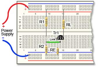
Fig. 2.1.2 Fitting the DC components.
Fit the transistor and the four resistors in place on the breadboard together with any necessary wire links (Do NOT fit any capacitors yet). Then after a thorough visual check that everything is correctly connected, connect the power supply, switch on and use a multimeter to check the voltages on collector, base and emitter of the transistor.
If the voltages are correct you have successfully designed the DC conditions. If there are any drastically wrong voltages, (e.g. more than 30% high or low) check that all the connections on the amplifier are correct, and that you have read the resistor colour codes correctly. Any smaller differences may need the value of one or more of the resistors changing.
Try to make collector voltage VC exactly half of the supply voltage VCC. If it already is, well done! If not (which is most likely) the first thing to check is that you have correctly calculated the values of RL and RE and fitted the nearest preferred value of resistor in both positions. If these resistors are OK, the base voltage probably needs correcting, as mentioned in "Estimate a value for base current" above. If the collector voltage is high, the base voltage will need increasing slightly (try changing R2 to the next higher preferred value). If the collector voltage is low, decrease the value of R2.
It is not unusual to have to ´tweak´ the values slightly in this way, as it is only possible to use preferred values of resistor rather than the exact calculated values. Make sure to note the effect of any changes you make, if you change a resistor value to increase a voltage, did it increase as expected? If not try to work out why. Remember the purpose of this exercise is to help you understand the effects of each of the components in the amplifier circuit − experiment and learn!


