Module 4.3
Amplifiers & Impedance
- After studying this section, you should be able to:
- Understand the advantages of controlling input and output impedance in amplifiers.
- Understand typical circuits used to increase amplifier input impedance.
- • JFET inputs.
- • The Darlington Pair.
- • Bootstrapping
- Understand typical circuits used to reduce amplifier output impedance.
- • Emitter Follower stages
Input & Output Imedance
The input and output impedances of an amplifier are very important parameters that affect the overall gain in multi-stage amplifiers. AC Theory Module 7.2 describes how correct matching reduces signal loss between the output of one amplifier and the input of the next in multi stage amplifiers. This section looks at practical methods of obtaining suitable input and output impedances where amplifiers interface with typical input and output devices such as microphones and loudspeakers.
Audio input sources, such as microphones, pick-ups, radio tuners etc. can have impedances ranging from a few hundred ohms to several thousand ohms. Where audio amplifier inputs may have to cater for a number of different input sources, switch selectable inputs to compensate for specific input devices, as described in Amplifiers Module 4.1.
The final (output) stage in a multi-stage amplifier has to drive a ‘transducer’, which will convert the electrical signal energy produced by the amplifier into some other useful form. For example the electrical waves produced by an audio amplifier will be converted into sound (air pressure) waves by a loudspeaker. A radio frequency (RF) amplifier in a transmitter may be used to drive an antenna (aerial), or a DC amplifier may be driving an electric motor or a relay. Any or all of these transducers may have quite low impedances and require considerable amounts of signal current or power, rather than large signal voltages to operate them. Therefore the output stage of an amplifier may need to have a low output impedance, much lower than would be possible using the common emitter voltage amplifiers described in Amplifiers Module 4.1 to 4.3.
This section describes some types of current and voltage amplifier circuits commonly used to modify input and output impedances. Power output stages are described in Amplifiers Module 5 .
FET Input Stage
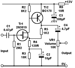
Fig. 4.3.2 High Impedance JFET Input Stage
Where very high impedance and low noise is required in an amplifier input, it is common to use a field effect transistor (FET) in an amplifier's input stage. Very high input impedance is obtainable with JFETs as its gate is voltage, rather than current operated. Therefore the JFET takes hardly any current from the device connected to the amplifier input. Even higher input impedances are available where MOSFETs with insulated gate construction (IGFETs) are used. Although FETs generally have less voltage gain and less bandwidth than BJT transistors they also create much less internally generated noise, which makes them ideally suited for use in the early stages of an amplifier, where good signal to noise ratio is important.
Operation
Because the input resistance of the JFET is extremely high, the input impedance of the circuit is approximately the value of R1, and as practically no current is flowing into the input, there is no potential across R1, therefore the gate of Tr1 is effectively at zero volts. To operate correctly, the gate of the N channel JFET must be more negative than the source, this is achieved by making the source of Tr1 positive. The signal applied to the gate will then vary the gate voltage and so vary the drain current through the JFET. The biasing of the JFET is set by R2 and R3. As JFET gain is not particularly high, extra gain is provided by the PNP transistor Tr2. The overall gain of the two-stage amplifier is set at approximately 11 by the negative feedback provided by R4 and R5.
Decoupling
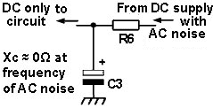
Fig. 4.3.3 Supply Decoupling
(From Fig 4.3.2)
In Fig 4.3.2, R3 is decoupled by C2 so that the bottom end of R4 is effectively at ground potential as far as AC is concerned, the value of C2 is not particularly large in this circuit, as the larger the value of electrolytic capacitor the more noise it will produce, and the aim of the circuit is to keep internally generated noise to a minimum. C1 and C4 coupling capacitors, (also relatively small values) provide isolation from any DC voltages present on any connected circuits. Using a very high value for R1 produces a high input impedance but the higher the value, the more prone the circuit will be to instability and oscillation. To prevent this possibility, effective decoupling from other circuits and the supply is necessary, decoupling here is provided by R6 and C3 as shown in Fig. 4.3.3.
The Emitter Follower
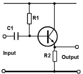
Fig. 4.3.4 Emitter Follower
Common emitter amplifiers generally have a medium to high output impedance, the value depending mainly on the value of load resistor in the final stage of amplification. Many typical transducers, such as loudspeakers, relays, motors etc. are inductive devices having a low impedance of only a few ohms.
Connecting such devices to the output of a voltage amplifier with a load resistance of several thousand ohms will result in poor impedance matching with practically the whole of the output being developed across the load resistor instead of across the load. One answer to this problem is to reduce the output impedance by using an emitter follower, which is a single transistor connected in common collector mode.
Common Collector Mode
This configuration uses the collector lead as the common connection for input and output. In the circuit (Fig. 4.3.4) the input to the transistor is connected between base and ground, and the output is connected across the load resistor between emitter and ground. Remember that with the collector connected directly to the supply, the collector is at ground potential as far as AC is concerned, because of the presence of large decoupling capacitors connected between supply and ground.
The common collector amplifier is called an emitter follower because the output, taken from the emitter is in phase with and ‘follows’ the input voltage at the base. In fact the base and emitter voltages are almost identical so the emitter follower has a voltage gain of 1 (in practice, slightly less) because of the 100% negative feedback created by the emitter load resistor not being decoupled, as would be the normal case in a common emitter amplifier. This causes the full amplitude of the output signal to be fed back to the base, giving a closed loop gain β of 1.
The emitter follower is therefore of no use as a voltage amplifier. It does however, have other very useful properties. Its current gain is large, and approximately equals the current gain (hfe) of the transistor. The input impedance of the circuit is high, 100KΩ or more being typical, although this will depend to some extent on the value of the base bias resistor R1 in Fig. 4.3.4, which is in parallel with the input resistance of the transistor, but this shunting effect can be reduced by ‘Bootstrapping’. The output impedance of the circuit is very low, typically in the region of 50Ω. Because of its use in matching relatively high output impedance voltage amplifiers to low impedance loads, the emitter follower may also be called a ‘Buffer Amplifier’.
The Emitter Follower as a Voltage Regulator
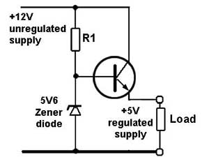
Fig. 4.3.5 Emitter Follower Voltage Regulator
Another use for the emitter follower is as a voltage regulator, and is useful in power supplies where a small voltage can be used to regulate a large current., as shown in Fig. 4.3.5. This circuit ensures that the regulated 5 volt supply remains at the correct voltage even if the 12 volt supply changes. An accurate five volts is also maintained for a range of currents drawn by the circuit being supplied. Regulation can be achieved just using a resistor and Zener diode combination but much higher currents can be handled when an emitter follower is used.
Notice in Fig.4.3.5 that the Zener diode has a voltage rating of 5V6 (meaning 5.6volts), this will maintain the base of the transistor at that voltage, and the emitter of the transistor at 0.6V below the base voltage, will be maintained at 5 volts. A small current maintaining the base voltage at 5.6V is therefore able to accurately control a much larger current flowing through the collector and emitter.
The emitter follower circuit is also the basis of many push-pull class B and class AB power output amplifier stages described in Amplifiers Module 5
The Emitter Follower Converted to a Darlington Pair
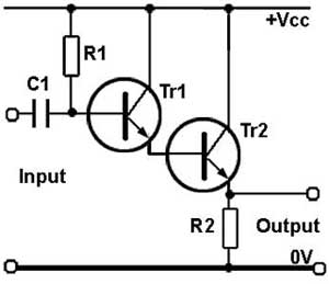
Fig. 4.3.6 The Darlington Pair
The effect of a high input impedance is to reduce the input current to the amplifier. If the input current for a given input voltage is reduced by whatever method, the effect is to increase the input impedance. The emitter follower has a high input impedance, but this may be reduced to an unacceptable level by the presence of the base bias resistor.
However another circuit, the compound or Darlington pair shown in Fig. 4.3.6 can greatly increase input impedance. By using one emitter follower (Tr1) to drive another (Tr2) the overall current gain becomes the product of the individual gains, hfe1 x hfe2 and can be typically 1000 or more. This greatly reduces the signal current required by the base of Tr1 and thereby dramatically increases the input impedance.
The Darlington Pair using Common Emitter Amplifiers
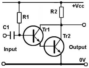
Fig. 4.3.7 Common Emitter Arrangement
The Darlington pair can also be used in common emitter mode, as shown in Fig. 4.3.7. Darlington transistors are also available as combined packages in both PNP and NPN types, complete with back emf protection diodes typically required when the Darlington configuration is used as a high current gain output device for switching high current inductive loads.
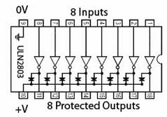
Fig. 4.3.8 The Darlington Integrated Circuit ULN2803
Darlington amplifiers are also available in integrated circuit form, such as the ULN2803, which contains eight high current, Darlington amplifiers with open collector outputs, for interfacing between TTL (5V) logic circuits and high current/high voltage (up to 500mA and 50V) devices. When pin 10 is connected to +V each output is diode protected for driving inductive loads against back e.m.f.
Bootstrapping
Bootstrapping (Using positive feedback to feed part of the output back to the input, but without causing oscillation) is a method of apparently increasing the value of a fixed resistor as it appears to A.C. signals, and thereby increasing input impedance. A basic bootstrap amplifier is shown in Fig. 4.3.8 where capacitor CB is the ‘Bootstrap Capacitor’, which provides A.C. feedback to a resistor in series with the base. The value of CB will be large, about 10 x the lowest frequency handled x the value of the series resistor (10ƒminR3).
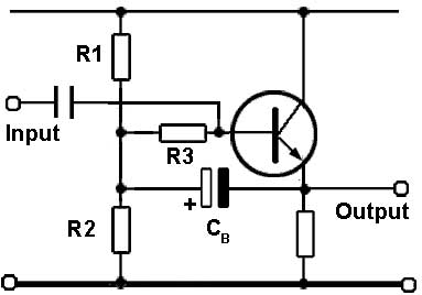
Fig. 4.3.8 Bootstrapping applied to an Emitter Follower
Although positive feedback is being used, which would normally cause an amplifier to oscillate, the voltage gain of the emitter follower is less than 1, which prevents oscillation.
In Fig. 4.3.8 the base of the emitter follower is biased from a potential divider via R3. By feeding the output waveform back to the left hand side of R3 the voltage at this end of R3 is made to rise and fall in phase with the input signal at the base end of R3.
Because the output waveform of the emitter follower is a slightly less amplitude than the base waveform (due to the less than 1 gain of the transistor) there will be a very small signal current waveform across R3. Such a small current waveform suggests a very small current is flowing; therefore the resistance of R3 must be very high, much higher than in fact it is. The input impedance of the amplifier has therefore been increased.
The effective A.C. value of R3 is increased by R3 ÷ (1 −Ao) where Ao is the open loop gain of the amplifier.
For example a 47KΩ resistor with bootstrapping would appear to be:

So if AO = 0.98 the apparent value of R3 would be 47 x 103 ÷ (1- 0.98) = 2,35MΩ
The main drawback of this method of increasing input impedance compared with other methods is that the use of positive feedback is likely to increase noise and distortion.


