Module 6.2
Comparators
- After studying this section, you should be able to:
- Describe how Op Amps can be used as Comparators.
- • Uses and Limitations.
- Understand Hysterisis as applied to Comparators.
- • Switching speed.
- • Effects of noise on switching.
- Describe the operation of a Schmitt Trigger Comparator.
- •The effect of positive feedback.
- •The control of Hysteresis.
- Understand typical Technologies used in Dedicated Comparator ICs.
- •Hysteresis and reference voltage.
- •Low Power v Switching Speed.
- •Typical Comparator Applications.
Using the Op Amp’s Open Loop Gain
The output of an op amp can swing positive and negative to a maximum voltage close to the supply rail potentials. For example, the maximum output voltage for the popular 741 op amp, when connected to a ±18V supply is ±15V.
Because the open loop gain of an op amp is extremely high however, (typically 10,000 to one million) means that without negative feedback, any input that creates a difference in voltage between the two input pins greater than ±150µV may be amplified by, for example 100,000 or more times, and drive the output into saturation; the output will then appear to be ‘stuck’ either at its maximum or minimum value.
Using the maximum open loop gain in this way can be useful when either dealing with extremely small (and low frequency or DC) inputs in instrumentation or medical applications, or for comparing two voltages, using the op amp as a comparator. In this mode the output will go to either a maximum high or minimum low level, depending on whether one input is just a few micro volts higher or lower than a reference voltage applied to the other input.
The Op Amp as a Comparator

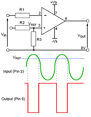
Fig. 6.6.1 Using an Op Amp as a Comparator
Basic op amp types such as the 741 will perform adequately as comparators in simple circuits, such as a temperature controlled switch that is required to switch on or off a circuit when the input voltage from a temperature sensor is higher or lower than a preset reference value.
In Fig. 6.6.1 a reference voltage is applied to the non-inverting input, whilst a variable voltage is applied to the inverting input. Whenever the voltage applied to pin 2 is higher than the reference voltage on pin 3 the output will be at a low voltage, only slightly higher than −Vs and if pin 2 is at a lower voltage than pin 3, the output voltage will be high, slightly less than +Vs.
However, standard op amps are designed for low power amplification purposes and if they are driven into, then out of saturation, it takes some time for the output voltage to recover and for the op amp to begin operating in a linear manner once more.
Op amps designed as amplifiers are not particularly suited to use as comparators especially where the input signals are changing rapidly in such applications as audio level sensors or analogue to digital converters. Another problem with the basic comparator arrangement illustrated in Fig 6.6.1 that is addressed by op amps specially designed as comparators rather than amplifiers, is that of noise. If there is a significant amount of noise on the input signal, especially when the input signal voltage is close to the reference voltage level, the high frequency voltage variations caused by the random nature of the noise will make the input signal voltage higher and lower than the reference voltage in rapid succession, causing the output to momentarily oscillate between its maximum and minimum voltage levels. However this problem is overcome in many dedicated comparators by applying hysteresis.
Hysteresis
This refers, in comparators and switching circuits, to the property of the output in switching to its high or low states at different input values. If a comparator switched its output at a single input voltage level as explained in the previous paragraph, or if the difference in the two levels provided by the comparator’s hysteresis is not wide enough, the switching from one of the two output conditions to the other could be very uncertain. Hysteresis can be applied to the op amp comparator and adjusted for a suitable hysteresis gap by using positive feedback in a circuit arrangement called the Schmitt Trigger.
The Schmitt Trigger

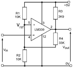
Fig. 6.6.2 The Op Amp Schmitt Trigger
The Schmitt Trigger circuit shown in Fig. 6.6.2 is an inverting comparator based on the LM339 quad comparator IC from Texas Instruments, with its reference value applied to the non-inverting input by the potential divider R1 and R2. This sets the reference voltage at half of the 5V single supply.
R3 is a pull-up resistor, which is used on the LM339 as this comparator has an open collector output, that is an output stage where the collector does not have an internal load resistor connected to supply. The reason for this is that it allows the output to have a wider range of DC voltages, rather than just being able to vary between supply and ground.
Positive Feedback
The resistor R4, connected between output and pin 5 (the non-inverting input) provides positive feedback to speed up output switching as follows. Suppose the voltage Vin on pin 4 is rising towards the reference voltage Vref on pin 5 and the output on pin 2 is high. Once Vin is slightly higher than Vref the output will start to fall towards 0V. A proportion of this fall in voltage is fed via R4 to pin 5 and so begins to reduce Vref increasing the difference between Vref and Vin. This causes the output to fall faster and because this fall is continually fed back to Vref the fall in the output voltage accelerates, causing a very rapid fall to zero volts. A similar action occurs when a high voltage on pin 4 falls to a lower value than pin 5, ensuring very fast output switching.
There is however, another action taking place; it was mentioned in the previous paragraph that a fall in the output voltage is fed back via R4 and causes a fall in Vref and likewise a rising output voltage will cause a rise in Vref, changing the reference point Vref depending on whether the output voltage is high or low. The difference between the high and low values of Vref is called the hysteresis of the circuit, and is an important property of the Schmitt Trigger.
Controlling the Hysteresis

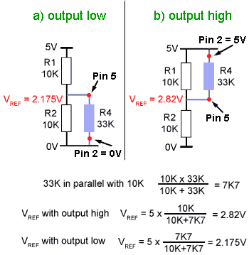
Fig. 6.6.3 The Effect of R4 on Hysteresis
Vref controls the point at which the output of the LM339 IC changes from low to high, or from high to low. By changing the value of Vref depending on whether the output is low or high introduces some hysteresis (a difference between the two switching points) into the circuit operation.
Vref is initially controlled by the choice of the potential divider values of R1 and R2. As these resistors have equal values of 10K, Vref should be at half the supply voltage (i.e. 2.5V). However the presence of the feedback resistor R4 introduces hysteresis by changing the value of Vref depending on whether the output is at its low or high state, as illustrated in Fig. 6.6.3a and Fig. 6.6.3b.
Fig 6.6.3a shows that when the output is low, pin 2 of the LM339 is at 0V and R4 is effectively connected between between Vref on pin 5 of the LM339 and 0V, effectively connecting R4 in parallel with R2, reducing Vref to 2.175V.
However, Fig 6.6.3b shows that when the output is high, R4 connects Vref on pin 5 of the LM339 to +5V, and so changes Vref to 2.82V as because R4 is now effectively in parallel with R1.
By choosing an appropriate value for R4, the amount of hysteresis (the change in Vref) can be varied to accommodate different anticipated levels of noise.
Dedicated Comparator ICs
For high speed comparisons many dedicated comparator op amps are available that will change their output state in less than 1µs. However, as is general with most electronic circuits, the faster the outputs change, the more power is consumed. Comparators of various speeds and different power consumption figures are available so that the ideal IC for a given application can be used, depending on whether power consumption or speed is more important.
Using methods similar in effect to those described above, high speed comparator integrated circuits with built in hysteresis are available, such as the LTC1541 from Linear Technology that has a built in hysteresis property of ±2.25mV to allow for noise on the input signal.
Comparator ICs are also available that have variable hysteresis to cope with different amounts of noise, and a built in precision reference voltage. Some comparators, such as the LMP7300 from Texas Instruments can also operate from very low single supply voltages and at extremely low currents. This makes them ideal for such applications as low battery voltage detectors in portable equipment.


