Module 6.4
Op amp Characteristics
- After studying this section, you should be able to:
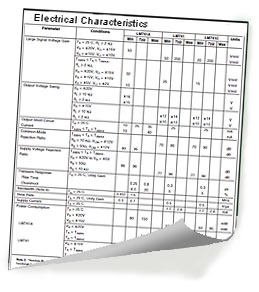
- Understand commonly published op amp characteristics.
- • Power suppliy requirements.
- • Open loop voltage gain.
- • Large signal voltage gain.
- • Gain bandwidth product.
- • Input offset current.
- • Maximum differential input.
- • Input resistance, Temperature coefficient.
- • Slew rate, Power bandwidth.

Supply Voltage
Two types of supply are used for op amps, the dual and single supply. Many op amps, especially older types use a dual supply (+VS and -VS) often in the 12 to 18V range. This allows a zero diffence between the input terminals to produce a 0V output and an output signal to swing both positive and negative with respect to ground.
Single voltage supplies have grown in popularity with the increase in portable (battery operated and/or automotive) devices where dual supplies, using multiple batteries are more expensive to implement. A zero difference between the input terminals on these devices will produce an output at half supply, allowing an output signal to swing between supply and ground.
Frequency Response
An important characteristic of any amplifier is its frequency response, in the ideal amplifier its frequency response should be infinite, it will amplify any and all frequencies equally. In practical amplifiers this is difficult/impossible to achieve, and not always desirable, but op amps have extremely wide, and easily variable bandwidths.

Fig.6.4.1 Typical Op Amp Frequency Response
Open Loop Voltage Gain
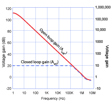
Fig. 6.4.1 shows the frequency response of a typical op amp (LMC660), which confirms that the open loop gain (with no feedback) at very low frequencies is huge. When Open loop Gain is quoted it refers to the maximum AC gain at very low frequencies.
It can be seen from Fig. 6.4.1 that the LMC660 for example has an open loop voltage gain of about 126dB (a voltage gain of nearly 2 million), but at frequencies above a few Hz, gain begins to fall rapidly at 20dB/decade until, at 1.4MHz the gain has reduced to 0dB, a voltage gain of x1.
Large Signal Voltage Gain
The large signal voltage gain is usually quoted in preference to the open loop voltage gain. This is the open loop voltage gain measured at DC with the amplifier producing a large (just less than maximum) voltage output, usually quoted in V/mV. Figures for large signal voltage gain can cover a wide range for a given op amp, depending on design variant and factors such as minimum or maximum operating temperature.
Closed Loop Voltage Gain
In practise the huge gain of an op amp is greatly reduced by applying an appropriate amount of negative feedback. In this way an impressively level response can be achieved, extending from DC (0Hz) to any frequency up to about 1MHz or more, as well as the added benefits of reduced noise and distortion. The blue dotted line shows the response of the op amp with negative feedback. The gain has been reduced to 20dB, a closed loop voltage gain (Acl) of x10, which has produced a flat response from 0Hz to about 140kHz.
Gain Bandwidth Product
As the closed loop gain and the small signal bandwidth of an op amp are closely related, the parameter ‘Gain Bandwidth Product’ is often used to better describe the possible combinations of gain and bandwidth. The graph of the open loop frequency response in Fig. 6.4.1 therefore, plots all those points where voltage gain x bandwidth = 1.4 million(Hz). For example, 140kHz bandwidth multiplied by a voltage gain of 10 also gives a Gain Bandwidth Product of:
10 x 140kHz = 1.4MHz
Note that bandwidth indicated by the Gain Bandwidth Product applies to small signals, but when large AC signals are involved, especially signals with fast rising and falling edges, the bandwidth may be further reduced by the Slew Rate. Then the Power Bandwidth becomes more relevant.
Maximum Differential Input
This is the maximum voltage that can be applied between the two inputs, on some devices this can be equal to the supply voltage, but on others it can be considerably less.
Input Resistance
This is the resistance looking into the input terminals with the amplifier operating without feedback (open loop). Typical resistances for bipolar devices are in the range of 1MΩ to 10MΩ. For FET and CMOS types, resistances are much higher, and range up to 1012Ω or more.
Input Offset Current
The currents flowing into the two inputs should ideally both be zero, but for practical op amps, although the input currents are still extremely small, they do exist and may also be different. Unequal currents cause different voltages at the inputs, and when this small difference in voltage is amplified, it causes the output to be other than zero. To overcome this effect an Input Offset Voltage can be applied between the inputs to correct the output voltage to zero. Typical values for bipolar op amps would be ±1mV ranging up to 15mV for FET types.
Temperature Coefficients
Both the input offset current and input offset voltage are affected by changes in temperature, and tend to drift higher as temperature increases. The temperature coefficient of input offset current is measured in nA or pA / °C while the temperature coefficient of input offset voltage is usually measured in µV/°C.
Slew Rate

Fig.6.4.2 Output Compensation
The Slew Rate of an op amp describes how fast the output voltage can change in response to an immediate change in voltage at the input. The higher the value (in V/µs) of slew rate, the faster the output can change and the more easily it can reproduce high frequency signals.
If a square wave is applied to the input of the op amp, the output should also be a square wave. However the fast rising and falling edges of the square wave can tend to cause the amplifier to oscillate for a short time after the rise or fall. To prevent this effect, the op amp’s internal circuitry contains a small amount of compensation capacitance that slows down the rate of change by acting as a CR time constant so that very fast transient voltages do not trigger oscillation, but this compensation also limits the slew rate of the op amp, as shown in Fig. 6.4.2.
In some op amps, because this compensation is internal, there is no way of altering the slew rate, but others use an external compensation capacitor, and therefore provide the means to control slew rate to some degree.
The slew rate also affects sine wave (and audio) signals as well as square waves. The rate of change of voltages in a sine wave is continually varying, it is changing at its fastest rate as the signal voltage crosses zero, and the rate of change falls momentarily to zero (no change) at both the positive and negative peaks of the wave. If the slew rate of the amplifier cannot keep up with the fastest rate of change of the signal, some distortion will be produced. Therefore, to be sure of amplifying large amplitude signals that are most likely to produce large (and fast) rates of voltage change, an op amp needs to have a sufficiently high value of slew rate to cope with the greatest possible rate of voltage change. If the largest possible voltage swing and the highest frequency of the signal are known, the minimum required slew rate for the op amp can be calculated using the formula:

Where f = the highest signal frequency (Hz) and Vpk = the maximum peak voltage of the signal.
For example if an op amp is to amplify a signal with a peak amplitude of 6 volts at a frequency of 40kHz, an op amp with a slew rate of at least 2π x 40 exp3 x 6 = 1.5V/µs would be required.
Power Bandwidth
Once the slew rate calculated as above for the large signal becomes equal or greater than the amplifier’s slew rate, ‘Slew Rate Limiting’ starts to occur, causing reduced gain and distortion of the signal. The highest frequency that can be used to amplify a full amplitude signal before ‘Slew Rate Limiting’ is the highest frequency limit of the Power Bandwidth. For example, in an op amp operating from a ±15V supply the power bandwidth would be specified as the frequency range in which a ±10V swing can be measured at the output with a total harmonic distortion of less than 5%. The Power Bandwidth is usually less than the small signal bandwidth indicated by the graph of the closed loop gain, and in many cases the major factor in specifying the amplifier bandwidth.


