Module 6.6
Op Amp Circuits
- After studying this section, you should be able to:
- Understand the operation of typical op amp circuits.
- • Voltage follower.
- • Differential amplifier.
- • Instrumentation amplifier.
- • Summing Amplifier: (DC level control, weighted resistor DAC, audio mixer).
- • Differentiator.
- • Integrator.
- • Active filters: (low pass, high pass, band pass).
Op Amp Circuits
Op amps are extremely versatile and have become the amplifier of choice for very many applications. The advantages of integration also allow op amps to be included in many application specific integrated circuits (ASICs) where, combined with other circuit elements, a chip can be designed to carry out a specific function, which for example, can vary from a dedicated tone control or a programmable filter network to a complete audio or communications system.
This section introduces some basic variations on the voltage amplifiers described in Module 6.3 that are commonly used in many circuits.
Voltage Follower
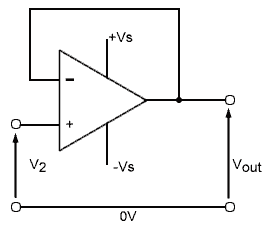
Fig.6.6.1 The Voltage Follower
The voltage follower shown in Fig. 6.6.1 looks rather like a non inverting voltage amplifier, but without its feedback and input resistors. The gain of a non inverting voltage amplifier would normally be described using the values of Rf and Rin by the formula:

In the voltage follower circuit however, both Rin and Rf are replace by simple conductors, and so both these values in the above formula will be extremely small, therefore the gain is 1. The voltage follower does not therefore, act as an amplifier, the output voltage ‘follows’ the input voltage, but the circuit does have some very useful properties.
Module 3.2 described how negative feedback can be used to increase the input impedance, and reduce the output impedance of an amplifier. The voltage follower uses 100% negative feedback that is effectively voltage derived and series fed, so the effect of the feedback on impedance is dramatic. The input impedance of the circuit is increased to typically many megohms (106 Ω) or even teraohms (1012 Ω) while the output impedance of the op amp remains very low, in the range of ohms to hundreds of ohms. As with any other negative feedback (NFB) amplifier noise and distortion are also reduced.
The voltage follower is therefore very useful as a buffer amplifier, that will reduce the loading effect on previous circuits and, because of its low output impedance will deliver more current to any following circuit.
Differential Amplifier
Fig. 6.6.2 shows a differential amplifier with a single output. This operating mode is a combination of both the inverting and the non-inverting amplifier. In this mode the output will be the difference between the two inputs, multiplied by the closed loop gain.
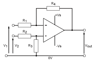
Fig.6.6.2 The Differential Amplifier
Setting the value of closed loop gain is normally achieved by choosing the ratio of the feedback and input resistors. In both the inverting and non-inverting amplifiers only one input was used, the other input being connected to ground.
In the differential amplifier however, both inputs are in use so two pairs of resistors are needed to control the gain, one pair for each input. It is important that the gains from both inputs are equal, otherwise the output would be equal to the voltage difference and the difference in gain.
Therefore in Fig. 6.6.2 for equal gain at each input R1 should equal R2 and R3 should equal R4.
One problem with the circuit in Fig. 6.6.2 is that, compared with the single input op amp mode, the input impedance is quite low. Another problem, especially where a gain greater than 1 is required, is that it becomes difficult to match the two gains accurately enough, even with close tolerance resistors because of unequal input currents, and the very small differences in input voltages that may be amplified to produce larger errors at the output.
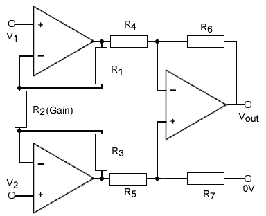
Fig.6.6.3 The Instrumentation Amplifier
Instrumentation Amplifier
Both of the problems mentioned in the previous paragraph, relating to input impedance and resistor matching, can be remedied by using a slightly more complex design, the Instrumentation Amplifier, shown in Fig. 6.6.3.
This circuit addresses the problem of low input impedance by using two non-inverting buffer amplifiers at the inputs to increase input impedance, and are designed with feedback resistors that give a closed loop gain of more than 1.
The problem of unmatched gains of the input buffer amplifiers is solved by the use of a shared input resistor (R2) so that the gain of both input amplifiers is set by just a single resistor.
The output amplifier can now have a gain of 1 and R4, R5, R6 and R7 can be all the same value. The problem of producing amplifiers and resistors with close tolerances and identical temperature coefficients is made easier if they are produced on a single wafer of silicon within an integrated circuit. Integrated circuit instrumentation amplifiers such as the INA114 from Texas Instruments are produced, looking very much like a single op amp but using a single resistor to set its gain.
Summing Amplifier
A summing amplifier is an extension of (usually) the inverting amplifier, which carries out a mathematical addition on a number of analogue signals (AC or DC) at its inputs. It can have a number of uses:
1. DC Level Control
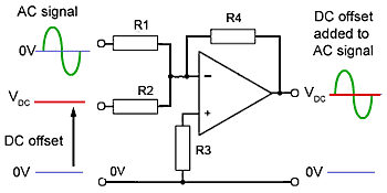
Fig.6.6.4 Adding a DC offset to an AC wave
By applying an AC signal to one of the summing amplifier inputs, and a DC voltage to the other, the DC voltage is added to the AC signal, changing the DC level of the AC wave. An example application of this could be the Y shift control on an analogue oscilloscope changing the vertical position of the waveform.
2. Digital to Analogue Conversion Using a Summing Amplifier
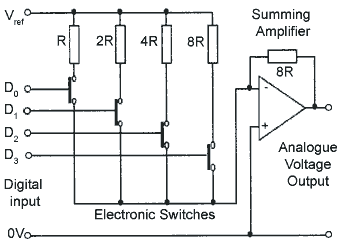
Fig.6.6.5 Digital to Analogue Conversion (DAC)
| D3 | D2 | D1 | D0 | Vout |
|---|---|---|---|---|
| 0 | 0 | 0 | 0 | 0V |
| 0 | 0 | 0 | 1 | 333mV |
| 0 | 0 | 1 | 0 | 666mV |
| 0 | 0 | 1 | 1 | 999mV |
| 0 | 1 | 0 | 0 | 1.333V |
| 0 | 1 | 0 | 1 | 1.666V |
| 0 | 1 | 1 | 0 | 1.999V |
| 0 | 1 | 1 | 1 | 2.333V |
| 1 | 0 | 0 | 0 | 2.666V |
| 1 | 0 | 0 | 1 | 2.999V |
| 1 | 0 | 1 | 0 | 3.333V |
| 1 | 0 | 1 | 1 | 3.666V |
| 1 | 1 | 0 | 0 | 3.999V |
| 1 | 1 | 0 | 1 | 4.333V |
| 1 | 1 | 1 | 0 | 4.666V |
| 1 | 1 | 1 | 1 | 4.999V |
The simplest type of Digital to Analogue Converter (DAC) uses a Summing Amplifier and a weighted resistor network as shown in Fig. 6.6.5 where resistors having values in the ratio 1, 2, 4 and 8 are fed from a stable reference voltage and can be individually switched into the input circuit of the summing op amp. The amplifier output will have 16 different voltage levels, depending on the 4 bit digital code applied to the inputs DO to D3. Supposing that Vref is 5volts, the output voltages for any possible input code would be as shown in the table in Fig 6.6.5.
3. Audio Mixer
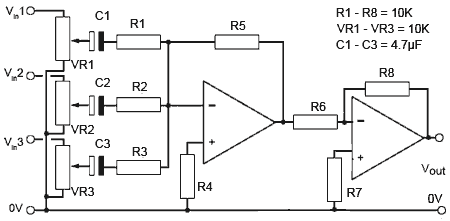
Fig.6.6.6 Audio Mixer Using a Summing Amplifier
The audio mixer shown in Fig. 6.6.6 uses a Summing Amplifier made from an inverting op amp with multiple input resistors (R1, R2 and R3), which together with the feedback resistor R5, add the individual signal input voltages at the inverting input of the op amp. In audio mixers R1 R2 and R3 will usually be the same value.
Because the summing amplifier used in stage one is based on an inverting amplifier, the signal at the output of stage one will be in anti-phase to the input signal, so to restore the signal to its original phase a second inverting amplifier is used. With R1 to R8 all of equal value, the gain of each stage, and therefore the overall gain, will be 1.
Active Filters & Wave Shaping
Adding an op amp to the passive wave shaping and filter circuits described in AC Theory Module 8 overcomes the problem that the gain of passive circuits is always less than 1, the output is always less than the input. This may be acceptable where only first order circuits (having only a single wave shaping or filter element) are used, but because the efficiency of the circuit is generally improved by using multiple circuit elements, for example using a low pass filter and a high pass filter in combination to make a band pass filter, second or even fourth order filters are often needed. In such cases the attenuation caused by the extra passive filter can cause an unacceptable reduction in signal amplitude.
With active filters and wave shaping circuits, op amps are used to overcome the losses due to passive components, making multiple (2nd, 3rd, 4th...etc. order) filters possible that have superior performance such as sharper cut off and a higher Q factor.
Op Amp Differentiator (or High Pass Active Filter)
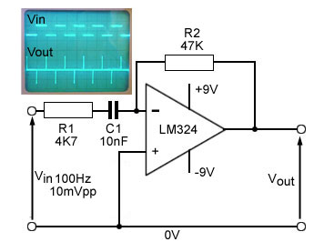
Fig.6.6.7 Op Amp Differentiator
When op amps are used in wave shaping circuits, the operation of the circuit uses the characteristics of the amplifier together with the properties of resistors and capacitors to obtain changes to the wave shape.
The circuit in Fig. 6.6.7 uses a CR time constant of C1 x R2 (10exp-9 x 470exp3) = 470µs to convert a square wave with a periodic time of 1/100Hz = 10ms, to positive and negative pulses. The time constant of a differentiator is shorter than the periodic time of the wave.
Temporarily ignoring R1, the operation is as follows:
The circuit illustrated in Fig. 6.6.7 is basically that of an inverting amplifier, but with the addition of a capacitor at the inverting input. If a steady voltage is applied to the left hand plate of C1 there will a voltage across C1 as the right hand plate is held at 0V (virtual ground) by the action of the op amp keeping the inverting input at the same voltage as the non-inverting input, which is connected to 0V. While the input voltage (a square wave) remains at a constant level, there will be no current flowing through C1 and therefore no current through R2. The output voltage will also be constant.
When the input voltage suddenly changes, there will be a sudden pulse of current into the capacitor as it quickly charges (due to the short CR time constant) to the new level. Supposing the input voltage has gone more positive, the op amp output will go negative to keep the inverting input at 0V. Notice that the active circuit produces a pulse in the opposite phase to that expected from a passive differentiator circuit due to the action of the inverting amplifier.
The op amp differentiator has produced good (though inverted) differentiation at low frequency, and the amplitude of the pulses depends on the rate of change of the input wave and also on the gain of the op amp. The gain will in turn depend on the ratio of R2 to the capacitive reactance (XC) of C1. However reactance reduces as frequency increases and so the gain of the op amp will increase with frequency. At some high frequency the reactance of C1 will have reduced to practically 0Ω and the gain of the op amp will be almost infinitely high. This will cause serious problems of high levels of noise together with instability. The circuit will start to oscillate uncontrollably. The purpose of R1 is to help prevent this instability, as the reactance of C1 reduces it will at some frequency fall below the resistance value of R1, and as C1 and R1 are in series the low value of XC becomes irrelevant and the ratio controlling the maximum gain will now be R2/R1.
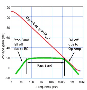
Fig.6.6.8 High Pass/Band Pass Active Filter Response
Active High Pass Filter
With both passive and active circuits the differentiator wave shaping circuit shown in Fig. 6.6.7 also acts as a high pass filter when the input is a sine wave. However with active versions of the circuit there is a significant difference to the passive circuit. Because the gain of the op amp falls off at some frequency due to its power bandwidth and slew rate limitations. This can affect its high frequency operation so that an active high pass filter will also behave to some extent as a band pass filter, with attenuation both below and above a central pass band as shown in Fig. 6.6.8. This can be a problem, but also an advantage if the frequencies at which the low and high corner frequencies are managed by the choice of appropriate component values.
Integrator/Low Pass Filter
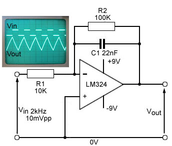
Fig.6.6.9 Op Amp Integrator/Low Pass Active Filter
In the op amp integrator circuit the capacitor is inserted in the feedback loop and creates a CR time constant with R1 at the inverting input. This point is held at virtual ground by the action of the op amp. As long as the input is at 0V there will be no current through the resistor R1, as the inverting input of the LM324 is at virtual ground.
C will be in a discharged state because of the presence of R2, which prevents C1 holding some charge from a previous state. If this were to happen the output (connected to the right hand plate of C1) could easily be driven to either +VS or −VS causing the op amp to ‘lock up’ and be unable to restore a normal output voltage.
If a square wave applied to Vin now enters its positive half cycle and produces a steady positive DC voltage at Vin a current will flow through R1 and begin to charge C1. Because the voltage at the junction of R1 and C1 (the inverting input of the LM324) is held at virtual ground, the voltage at the op amp output, (connected to the right hand plate of C1), will begin to fall at a rate controlled by the CR time constant. The output voltage will continue falling, trying to reach a negative voltage, equal and opposite to Vin This action causes a relatively linear negative going ramp at the output until (well before the end of one time constant), the input square wave suddenly changes polarity.
Changing the voltage at Vin back to its lower level at the start of the negative going half cycle of the input square wave will cause C1 to begin to discharge, and to keep the inverting input at 0V, the voltage at the op amp output will begin to increase in a linear manner. This continues until the input suddenly goes positive once more at the start of the next cycle.
To produce a linear ramp on the output triangular waveform, the CR time constant of the integrator circuit should be similar to, or longer than half the periodic time of the input wave. In the case illustrated in Fig. 6.6.9, a time constant R1 x C1 (10exp3 x 22exp-9) = 220µs converts a 1kHz square wave with a periodic time of 1/2exp3Hz = 500µs/2 = 250µs into a reasonably linear triangular wave.
2nd Order Active Filter
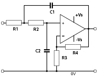
Fig.6.6.10 2nd Order Low Pass Active Filter
Fig. 6.6.10 shows a 2nd order Sallen-Key low pass filter with a double CR low pass filter network. Such filters are normally designed using graphs and tables of component values for particular frequencies, as the design of multi order filter networks using mathematics is extremely complex and time consuming. An alternative is to use multi stage programmable filters, which contain several active filters in a single integrated circuit. These are of two main designs, either switched capacitor or analogue filters. Fig 6.6.11 illustrates a typical analogue example, the UAF42 from Texas Instruments It contains four separate analogue active filters that can be digitally programmed to create any combination of the four main filter types.
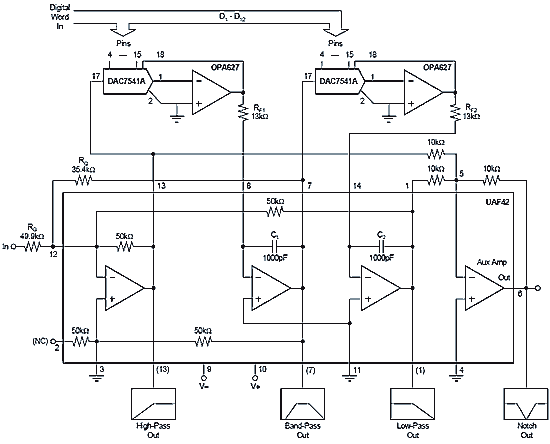
Fig.6.6.11 UAF42 Digitally programmable Analogue Filter IC by Texas Instruments


