Module 5.8
An Arithmetic and Logic Unit
- After studying this section, you should be able to:
- Understand Stuff.
- Understand the operation of a basic ALU circuit.
- • Stuff.
- Understand the relationship between Binary Arithmetic and digital circuits.
- • Twos complement arithmetic.
- • Adders & error flags.
- • Logic operations with shift registers.
- Use Free Stuff. .
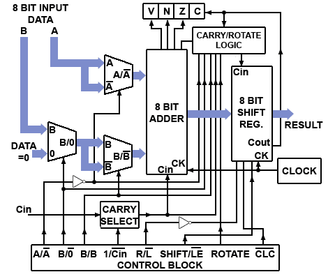
Fig. 5.8.1 ALU Block Diagram
Connecting Digital Circuits Together.
Digital Electronics Modules 2 to 5 have described how basic logic gates may be combined, not only to perform standard logic functions, but to build circuits that can perform complex logic tasks. Both small scale integrated (SSI) and medium scale integrated (MSI) chips are available in many forms, that can be directly connected together to make very complex circuits. It is this inter-connectivity that makes digital electronics so powerful and so versatile.
The standard circuits described in modules 2 to 5, both combinational and sequential, can be used to perform arithmetic operations such as addition, subtraction and counting, as well as logical operations such as combining data sources (multiplexing) and shifting bits left or right within a binary word.
As explained in Module 1, binary arithmetic is normally carried out electronically by using twos complement notation. The most common and versatile method of carrying out such operations is in an Arithmetic and Logic Unit (ALU), a circuit that forms the heart of any calculating or computing system.
The Arithmetic and Logic Unit
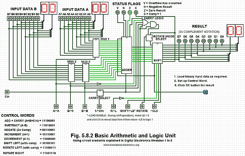
A simplified ALU is illustrated in Fig 5.8.1, which uses an arrangement of both combinational and sequential circuits from those described in modules 2 to 5. Their purpose is to perform the basic (though still complex) binary arithmetic described in Module 1.
Data passing through the ALU circuit does so on a system of buses, shown by the broad arrows in Fig. 5.8.1. These buses consist of groups of wires (usually as 8 parallel bits in simple systems) each carrying a single byte of binary data. In this system, data word A is the primary data source, and data word B is the secondary data source that may be added to, or subtracted from word A.
The ALU can also perform other operations. It can increment, add 1 to word A, or decrement, subtract 1 from it. By complementing (inverting) the logic value of individual bits of the data word A and adding 1 to the result, it is possible to use twos complement arithmetic to perform subtractions.
The shift register at the ALU output can also perform a ‘logical shift-left’ on word A by shifting the 8 bits consecutively into the carry bit, alternatively the shift register can create a rotating pattern of bits, rotating left, and using the carry bit as a ninth bit in the sequence, or rotate the 8 bits right ignoring the carry bit. Any of these functions can be selected by the control block, using various combinations of the eight control lines shown in Fig. 5.8.1.
Putting the correct pattern of 1s and 0s (the control word) on the control lines will cause the ALU to perform the required arithmetic or logical operation on the data being input at A and B. With a control word of 8-bits, this could potentially allow up to 256 different combinations, or control words, which would be more than ample, even for very complex microprocessors or micro controllers. However this basic ALU needs only eight control words to control the different operations available.
To see the ALU operate as described below, you can download our free, fully interactive Logisim ALU circuit (assuming you have the free Logisim Digital Simulator installed on your desktop or laptop computer), see our extra Logisim page for details.
The Component Parts
Any of the component parts of the Logisim design can be examined in detail by double clicking on the component (in simulation mode). To return to the main document, click ‘main’ in the component menu at the left of the screen.
Note: In this section the tilde character ~ is used where necessary to indicate NOT (e.g. ~LE = LE) to match the usage in the Logisim simulations.
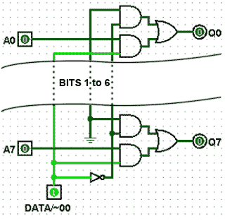
Fig. 5.8.4 MUX 2
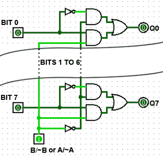
Fig. 5.8.3 MUX 1 and MUX 3
Multiplexers
MUX 1 and MUX 3 are identical 8 bit multiplexers that select either the input data word A (MUX 1) or data word B (MUX 3) or their internally generated complement, as shown in Fig. 5.8.3.
MUX 2 is a similar design but selects either the data word B or the zero value 00HEX , as shown in Fig. 5.8.4.
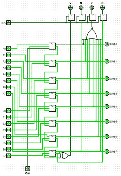
Fig. 5.8.5 The ALU Adder Component
8-Bit Adder
The adder component is an 8-bit ripple carry adder; real ALUs would normally feature a ‘carry-look-ahead’ adder, allowing for high-speed operation. However for this example the much simpler ripple carry adder is adequate, as the operation is totally manual.
The adder component is illustrated in Fig. 5.8.5 and consists of eight full-adder circuits with additional logic consisting of an XOR gate to detect overflow errors, and an 8-input NOR gate to detect a zero result.
Negative results are indicated by sampling the most significant bit of the ‘sum’ output, and a ‘carry’ is indicated by sampling the carry output of the most significant full adder.
Four D type flip-flops are used as ‘flag’ outputs to indicate the current state of the ALU after each operation.
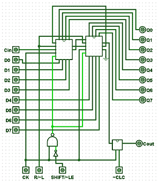
Fig. 5.8.6 The ALU Shift Register Component
The Shift Register
This component uses two 4-bit shift registers (from Module 5.7) connected in cascade as shown in Fig. 5.8.6. Inputs are provided for clock pulses, (CK), a right/left shift control (R/~L) and an input to control whether the shift register is in shift, or load-enable modes (SHIFT/~LE).
If ~LE is chosen temporarily during shift operations, the shift register can be reloaded from the data placed on the 8-bit ‘Data A’ and ‘carry-in’ (CIN) inputs. This action is synchronised to the CK pulse by the external NAND and NOT gates connecting the SHIFT/~LE input to the two ~LOAD inputs of the 4-bit shift registers.
An additional JK flip-flop (mimicking a D type flip-flop) is placed between the ‘serial-right’ output of the shift register and COUT to allow the ‘clear carry’ input (~CLC) to clear the carry flag.
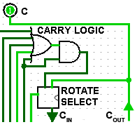
Fig.5.8.7 ALU Carry Logic
Carry Logic and Rotate Select
The carry logic circuit shown in Fig. 5.8.7 prevents the carry flag being set in rotate right mode, as bits rotate from bit 0 and re-enter the shift register at bit 7, therefore allowing correct carry flag operation in both left and right rotate modes.
When the ROTATE input is at logic 1, the Rotate Select circuit in Fig 5.8.7 allows COUT from the shift register to be fed back to the shift register CIN input for continuous bit rotation.
ALU Operation
Addition
To perform an addition, input data B is added to A. This is achieved by putting logic 1 on the control inputs of multiplexers 1, 2 and 3. This causes data A and B to be applied to the adder inputs. Also, to allow any carry bit from the CIN input to be included in the addition, the 1 bit carry multiplexer must have logic 0 on its control input. The shift register is only used as a PIPO register in addition mode, so its input lines R/~L and ROTATE must be at logic 0. SHIFT/~LE must also be at logic 0 to enable parallel loading of the shift register, which will hold the result of the addition (A plus B) after the application of a single CK pulse.
The Status Flags
The Flag flip-flops are special outputs from the adder circuit. They consist of four separate D type flip-flops, each of which can be set to 1 or cleared to 0. They are set or cleared by the result in the adder. They signal, or ‘flag’ to the user, that a particular event has occurred.
The Carry flag (C)
The carry flag will be set if the result of any arithmetic or logic event causes a logic 1 to be carried over from bit 7 into the ‘carry bit’, (which is the carry flag). The carry flag can be cleared at any time by making the ‘clear carry’ input (~CLC) logic 0.
The Overflow flag (V)
When carrying out twos complement arithmetic, errors can occur if large numbers are involved. For example if two positive numbers less than 12710 are added and produce a negative result (any value greater than 12710). This would cause the sign of the result (indicated by bit 7) to be wrong. The overflow flag gives an indication that an error has occurred by being set to 1 to indicate an ‘overflow error’. An error is sensed and the overflow flag is set when either of two conditions occurs.
There is a carry of logic 1 from bit 6 to bit 7 of the result, but the carry flip-flop is not at logic 1.
There is no carry from bit 6 to bit 7 of the result, but the carry flip-flop is at logic 1.
By using the carry-out from bit 6 and the carry-out from bit 7 of the result as inputs to an XOR gate, the output of the gate will be set to logic 1 for either of the above error conditions, signalling an overflow error at the overflow (V) flag.
The Zero flag (Z)
This flip-flop is set when every bit of the result is zero.
The Negative flag (N)
A negative result, i.e. bit 7 = 1 sets this flip-flop to logic 1.
The Flag Register
The status flags are individual bits of a register called the Flag Register, and are operative not only when the ALU is in addition mode, but also in all other arithmetic modes, the C flag is also operative in shift and rotate left modes. In microprocessors the flag register not only indicates ALU results, but can also be used in decision-making. For example the ALU can be used to compare (by subtracting) two values and take various actions depending on the state of particular flags; e.g. after comparing two values, A and B, an action may be taken if A = B, indicated by the zero flag being set to 1, otherwise (if the zero flag is set to 0) take no action.
Subtraction.
Subtraction is performed using twos complement arithmetic. That is, to subtract B from A, input B is complemented and 1 added to the complemented value to form the twos complement. Then the twos complement of B is added to A in the adder to find the result. To achieve this action with data A and data B present at the inputs, logic 1 is applied to the control inputs of MUX 1 and MUX 2. MUX 3 has logic 0 applied to its control input to complement data B, while the CARRY MUX has a logic 1 applied to its control line so that the carry-in (CIN) to the adder is forced to logic 1. This adds 1 to the result so that the twos complement of data B is added to data A. The result at the adder output is a twos complement number representing A - B. The flags are again set by the result as in the addition operation.
Counting with the ALU
Although the ALU does not include a binary counter circuit, it can also be used to count, by INCREMENTING or DECREMENTING, i.e. to add 1 to data A (incrementing), or subtract 1 from data A (decrementing). To count using this method would normally be carried out using (machine code or assembly language)software. A typical use could be to initiate a time delay by loading the ALU with some number, and then execute a looping routine to count down to zero by repeatedly decrementing data A. The zero result would be detected from the zero flag being set. However this would not be a common method, as the ALU (and therefore the CPU) would be occupied during the delay, and therefore not usable for other purposes. Most computer systems would also have dedicated counters for implementing similar time delays.
Incrementing.
Data A can be incremented if logic 1 is applied to the control inputs of MUX 1 and MUX 3. This will add B to A, with data B made zero by applying logic 0 to the control input of MUX 2. The 1 that must be added to data A is supplied by making the control input of the CARRY SELECT block logic 1, causing the carry input to the adder to be logic 1. The result at the adder output is therefore A + 1, again the flags are set by the result.
Decrementing.
To decrement data A, 1 must be subtracted from A. Because the ALU uses twos complement arithmetic, the twos complement of 1 added to A will in effect subtract 1 from A.
The twos complement of 1 is minus 1, which in 8-bit twos complement notation is 111111112. Therefore to subtract 1 from data A, data B must equal minus 1 (all bits = 1). To do this, and to make sure that the correct result is not changed by any data appearing on the data B input, logic 0 is applied to the control input of MUX 2 to make sure all data B bits = 0.
Logic 0 is also applied to the control input of MUX 3. This inverts data B, (which is 000000002) to give 111111112 at the adder input.
MUX 1 must have logic 1 on its control line, to apply data A to the other adder input. The adder’s carry input is set to 1 by applying logic 0 to the control line of the CARRY MUX. This ensures that, provided there is no carry-in on the CIN input, the correct result at the adder output will be A − 1.
Negation
Negation is simply the inverse of a value; therefore any value and its inverse will add to produce zero. In binary arithmetic the additive inverse of a value is its twos complement. The ALU can be used to negate (find the twos complement of) data A by complementing data A and then adding 1. This involves a similar process to decrementing, except that data B is treated differently, as follows:
The control input of MUX 1 is set to logic 0, which complements data A, also data B is made zero by putting logic 0 on MUX 2 control, and logic 1 on MUX 3. The Carry Select control input is set at logic 1, to add 1 to data A in the adder.
The shift register is used as a simple PIPO register by applying logic 0 to the three shift controls and logic 1 to the ~CLC input to make sure the carry is not cleared. This gives a final result of A+1, which is the twos complement of A.
The Shift Operations
Shift operations are controlled by the four lower order control lines, R/~L controls the direction of shift or rotation, SHIFT/~LE has the dual purpose of enabling the shift operations if logic 1 is applied, or acting as a LOAD ENABLE when at logic 0, allowing the shift register to be loaded or reloaded with appropriate data. Each action of the shift register (shift, rotate or load) is actuated by a single CK pulse. Also note that the shift register in this design does not affect the V, N or Z flags.
Shift Left (with Carry)
In this mode (with control word 10100101) input data B is kept at zero and, after the shift register is loaded by temporarily making SHIFT/~LE logic 0 to move data from input A into the shift register, shift is enabled by returning SHIFT/~LE to logic 1, and both ROTATE and ~CLC are disabled. The data in the shift register will now shift one bit to the left with each CK pulse applied. This appears to multiply the value of the data by two for each shift left, but it is a very limited multiplication operation, because the result is reduced each time the left most bit is lost as it passes through the carry bit. This action is therefore considered a logical, rather than an arithmetic shift.
Rotate Left (with Carry)
If rotate is activated by applying logic 1 to the ROTATE control input with SHIFT/~LE and ~CLC also at logic 1, the data being shifted left from bit 7 and through the carry flag, is returned via the CIN input of the shift register to re-enter at bit 0 by the action of the ROTATE MODE SELECT data selector.
Rotate Right
When data in the shift register is rotated right, it leaves the register via bit 0 and is returned directly to bit 7 via an internal link, without passing through the carry flag.
There are a number of other operations, such as performing 8 bit logic functions, commonly found on microprocessors that this ALU is not designed to do. The purpose of this design is to illustrate how the circuits described in Digital Electronics Modules 1 to 5 are really just part of a bigger picture, they can be inter-connected in many ways to make many different circuits. This ALU design is one example, but how you use what you learn from the pages of learnabout-electronics and how you fit that knowledge into your own imagination is up to you.


