
Module 4.1
Junction Field Effect Transistors
- Section 4.1 Field Effect Transistors.
- • FETs JFETs, JUGFETs, and IGFETS
- • The JFET.
- • Diffusion JFET Construction.
- • Planar JFET Construction.
- • JFET Circuit Symbols.
- Section 4.2 How a JFET Works.
- • Operation Below Pinch Off.
- • Operation Above Pinch Off.
- • JFET Output Characteristic.
- • JFET Transfer Characteristic.
- • JFET Video.
- Section 4.3 The Enhancement Mode MOSFET.
- • The IGFET (Insulated Gate FET).
- • MOSFET(IGFET) Construction.
- • MOSFET(IGFET) Operation.
- • MOSFET (IGFET) Circuit Symbols.
- • Handling Precautions for MOSFETS
- Section 4.4 The Depletion Mode MOSFET.
- • Depletion Mode MOSFET Operation.
- • MOSFE (IGFET) Circuit Symbols.
- • Applications of MOSFETS
- • High Power MOSFETS
- Section 4.5 Power MOSFETs.
- • MOSFET Calculations.
- Choosing a MOSFET.
- Section 4.6 MOSFET Switches.
- • Design and Build typical Mosfet Switch Circuits.
- Section 4.7 FET Quiz.
- • Check your understanding of Field Effect Transistors.
Field Effect Transistors
Although there are lots of confusing names for field effect transistors (FETs) there are basically two main types:
1. The reverse biased PN junction types, the JFET or Junction FET, (also called the JUGFET or Junction Unipolar Gate FET).
2. The insulated gate FET devices (IGFET).
All FETs can be called UNIPOLAR devices because the charge carriers that carry the current through the device are all of the same type i.e. either holes or electrons, but not both. This distinguishes FETs from the bipolar devices in which both holes and electrons are responsible for current flow in any one device.
The JFET
This was the earliest FET device available. It is a voltage-controlled device in which current flows from the SOURCE terminal (equivalent to the emitter in a bipolar transistor) to the DRAIN (equivalent to the collector). A voltage applied between the source terminal and a GATE terminal (equivalent to the base) is used to control the source - drain current. The main difference between a JFET and a bipolar transistor is that in a JFET no gate current flows, the current through the device is controlled by an electric field, hence "Field effect transistor". The JFET construction and circuit symbols are shown in Figures 1, 2 and 3.
JFET Construction
The construction of JFETs can be theoretically quite simple, but in reality difficult, requiring very pure materials and clean room techniques. JFETs are made in different forms, some being made as discrete (single) components and others, using planar technology as integrated circuits.
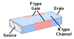
Fig. 4.1.1 Diffusion JFET Construction
Fig. 4.1.1 shows the (theoretically) simplest form of construction for a Junction FET (JFET) using diffusion techniques. It uses a small slab of N type semiconductor into which are infused two P type areas to form the Gate. Current in the form of electrons flows through the device from source to drain along the N type silicon channel. As only one type of charge carrier (electrons) carry current in N channel JFETs, these transistors are also called "Unipolar" devices.
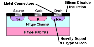
Fig. 4.1.2 JFET Planar Construction
Fig. 4.1.2 shows the cross section of a N channel planar Junction FET (JFET) The load current flows through the device from source to drain along a channel made of N type silicon. In the planar device the second part of the gate is formed by the P type substrate.
JFET Circuit Symbols
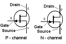
Fig. 4.1.3 JFET Circuit symbols
P channel JFETs are also available and the principle of operation is the same as the N channel type described here, but polarities of the voltages are of course reversed, and the charge carriers are holes.
Notice in the JFET circuit symbols shown in Fig. 4.1.3 that the arrowhead on the gate connection always points towards the negative connection, indicating the polarity (either P or N channel) of the channel.