Module 3.1
Negative Feedback & Gain
- After studying this section, you should be able to:
- Understand the basic principles of NFB as applied to amplifiers.
- • Open loop gain.
- • Closed loop gain.
- • The relationship between β and gain.
- • Reasons for using Negative Feedback.
Why NFB is needed in amplifiers
Transistors cannot be manufactured to have a closely controlled value of current gain hfe therefore it should not be possible to build a number of examples of the same amplifier circuit, all having the same gain. In addition the gain of a transistor varies with temperature, and even has different gain at different frequencies. All of these factors would make transistor amplifiers totally unreliable and impossible to make in large numbers. The main reason that this situation does not exist, and transistor amplifiers have become the mainstay of the electronics industry is the introduction, very early in the transistor’s history, of negative feedback.
Principle of NFB
The principle of negative feedback is that a portion of the output signal is fed back to the input and combined with the input signal in such a way as to reduce it. This reduces the overall gain of the amplifier but also introduces a number of benefits, such as reducing distortion and noise, and widening the amplifier’s bandwidth.
Problems with NFB
Introducing feedback within a system can also introduce the possibility of instability; in amplifiers the signal will normally undergo a phase reversal of 180 degrees between input and output but reactive components such as capacitors and inductors, whether actual components or ‘stray’ capacitance and inductance, can introduce unwanted phase changes at particular (usually high) frequencies. If these additional changes add up to a further 180 degrees at any frequency where the transistor has a gain of more than 1, the application of negative feedback may become positive feedback. Instead of reducing gain this will increase it to the point where the amplifier will become an oscillator and produce unwanted signals. Negative feedback must therefore be designed to maximise the benefits mentioned above, without creating unwanted problems.

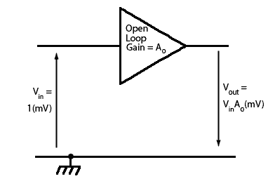
Fig. 3.1.1 Open Loop Mode
The Amplifier in Open Loop Mode
Fig. 3.1.1 shows a phase reversing voltage amplifier with gain in open loop mode i.e. with no feedback which can be called Ao (Amplification in open loop mode). Supposing an input signal of 1mV is applied, then the output will be an inverted (anti-phase) signal with an amplitude of 1mV x Ao = Ao(mV).

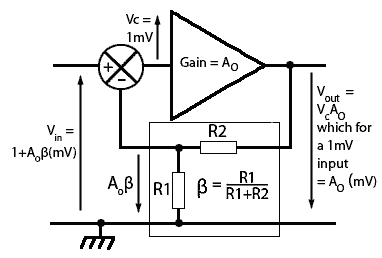
Fig. 3.1.2 Closed Loop Mode
The Negative Feedback Amplifier in Closed Loop Mode
A basic negative feedback arrangement is shown in Fig. 3.1.2 where the phase reversing amplifier has a fraction of its output (Vout) fed back and added to the input (Vin) so as to reduce the amplitude of the input signal. The arrows show the relative polarity of the signals and it can be seen that the output and the feedback signals are in anti-phase to the input signal. The fraction of the output signal to be fed back is controlled by the potential divider (β) and this fraction is added to the input signal in anti-phase,so that it is in effect, subtracted from the input signal (Vin) to give a combined signal (Vc) that is reduced in amplitude before being fed to the actual input of the amplifier.
The gain of the amplifier, excluding any feedback, is Ao so that, for example, every 1mV applied across the circuit’s input terminals, the amplifier will produce a phase-reversed signal of Ao x 1mV across the output terminals.
The feedback circuit comprising R1 and R2 will feed back a fraction (β) of output Vout which = Ao, so that Ao x βmV (Aβ) will be added in anti-phase to the 1mV signal to produce a reduced input signal of Vc.
The signal source Vin driving the amplifier must therefore deliver not 1mV but 1+AβmV to produce the same amplitude of output. Therefore the overall gain of the amplifier with negative feedback is reduced and is now called the closed loop gain (Ac).
Negative Feedback Formula
The voltage gain of any amplifier can be described by the formula:

Because in the closed loop negative feedback amplifier (Fig. 3.1.2):
Vout = Ao
and
Vin = 1+Aoβ
the closed loop gain (Ac) can also be described by the standard NFB formula:

Negative feedback amplifiers are designed so that the open loop gain Ao (without feedback applied) of the amplifier is much greater than 1, and so the 1 in the formula becomes insignificant. The closed loop gain (Ac) can therefore be approximated to:

The effect of NFB on amplifier Gain
This is of great significance because it means that, once negative feedback is applied, the closed loop gain Ac depends almost exclusively on β, which in turn depends on the ratio of the potential divider R1, R2.
Example:
The amplifier in Fig 3.1.2 uses the following feedback resistors:
R1 = 1kΩ
R2 = 10kΩ
Therefore:
β = R1 / (R1+R2) = 0.0909 = 1 / 11
and as the closed loop gain Ac = 1/β then:
Ac 1 / 0.0909 = 11
Testing this approximate result against the full formula for the closed loop gain:
Assuming an open loop gain of 1000 and β = 1 / 11 the closed loop gain Ac should be 11
Compare this result with the full formula for closed loop gain by entering the following data into your calculator:
1000 / (1+ 1000* 11−1) = 10.88
So the closed loop gain of the amplifier is actually 10.88, but a gain of 11 is close enough to this figure for any practical purposes.
How would a change in the open loop gain of the amplifier affect the closed loop gain with the same negative feedback applied?
To see the effect of large changes in open loop gain, try the same calculation but this time make the open loop gain Ao = 5000
Enter this data into your calculator: 5000 / (1+ 5000* 11−1) = 10.97
So for a 400% increase in the open loop gain, the closed loop gain has changed by only 0.8%
This means that the gain no longer relies on the variable, temperature dependent and non-linear gain characteristics of the transistor, but on a minimal two resistor network that has a linear temperature coefficient and an easily predicted β value.


