Module 3.2
Negative Feedback & Impedance
- After studying this section, you should be able to:
- Give reasons for using DC and AC negative feedback in amplifiers.
- Describe the effects of implementing Negative Feedback (NFB) on the input and output impedance of amplifiers:
- • Voltage Derived, Series Fed.
- • Current Derived, Series Fed.
- • Voltage Derived, Parallel Fed.
- • Current Derived, Parallel Fed.
- Understand how DC and AC negative feedback may be applied in amplifiers.
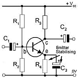
Fig 3.2.1 Emitter Stabilising Components.
DC Negative Feedback
DC negative feedback, is used in stabilising the biasing of amplifiers against drift due to thermal effects etc. Because negative feedback amplifiers often use direct coupling and may have several stages of amplification, stable bias conditions are essential. Very small changes in bias in an early stage can become major problems as the error is amplified in following stages.
AC Negative Feedback
As described in Amplifiers Module 3.1 AC negative feedback (NFB) in amplifiers feeds back a fraction of the output signal to the input in such a way that it subtracts from the input signal, reducing overall gain.
In its simplest form NFB can be applied to a single stage amplifier by changing the arrangement of emitter stabilising components shown in Fig. 3.2.1 as explained in Amplifiers Module 2.4
Using multi stage amplifiers overall gain can be greatly increased, as the overall gain is the product of the individual amplifier stages. Amplifiers Module 3.1 explained how it is possible to design an amplifier with NFB that has an exact amount of gain and can be simply set by the choice of two resistor values.
Controlling Input & Output Impedance with NFB
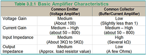
The way that negative feedback is derived from the output of the amplifier and applied to the input can be used to modify the amplifier’s input and output impedances so that impedance matching is maximised. In single stage amplifiers, input and output impedance depeds mainly on the amplifier configuration used. Table 3.2.1 compares basic input and output impedances for single stage voltage amplifiers (common emitter) and current/buffer amplifiers (common collector or emitter follower).
However with multi-stage amplifiers, different types of negative feedback can be employed to control the values of input and output impedance. The diagrams below show four basic methods of implementing NFB and how in each case, the feedback is derived from the output and is applied to the input.
Fig. 3.2.2 Voltage Derived, Series Fed NFB
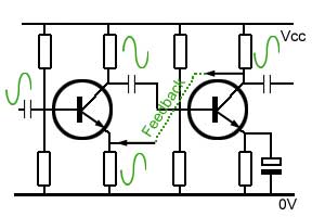
In Fig. 3.2.2 the feedback is derived from the collector voltage, which effectively reduces the output impedance of the amplifier. Applying the feedback to the emitter circuit of the input stage, which is in phase with the base signal, the feedback waveform on the emitter reduces the current into the base, so effectively increasing the input impedance.
Fig. 3.2.3 Current Derived, Series Fed NFB
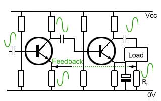
Fig. 3.2.3 shows the feedback applied in series again, increasing the input impedance of the amplifier as in Fig.3.2.2. In this circuit the feedback is derived from a resistor (Rf) connected in series with the amplifier load current in order to maintain the correct phase relationship with the emitter signal of the input transistor; the extra resistance here will effectively increase the output impedance.
Fig. 3.2.4 Voltage Derived, Parallel Fed NFB
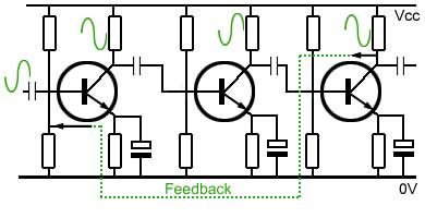
With voltage derived parallel fed NFB both input and output impedances are reduced. In Fig.3.2.4 an intermediate stage has been included maintaining the correct 180° phase relationship between the output collector voltage and the input voltage waveform.
Fig. 3.2.5 Current Derived, Parallel Fed NFB
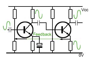
When this configuration is used, the input impedance is reduced and the output impedance increased.
The choice of which of these four feedback connections is used depends on a number of factors, including the required effect on input and output impedance, and the phase relationship between the feedback source and the point of application.
Problems with negative feedback.
Designing a multi stage amplifier using negative feedback has the advantages of being able to closely control the gain, independent of individual stage gains, and in addition being able to control the input and output impedances of the amplifier. There is however a practical limit to the amount of NFB applied in any particular circuit.
There will inevitably be phase shifts generated within the feedback loop, especially where capacitors are used in conjunction with resistors, as is the case with the coupling capacitors and bias resistors in each of the examples in Figures 3.2.2 to 3.2.5. Such combinations will form filter networks that produce phase shifts at some particular frequency. If these unwanted phase shifts add up to 180° at any frequency where the amplifier has a gain of more then 1, then the circuit becomes unstable and acts as an oscillator.
It is therefore usual for amplifier designs to avoid the use of coupling and decoupling capacitors where possible to avoid the problems of instability at low and medium frequencies. Where such a problem may still exist at high frequencies it may be necessary to include extra reactive components (capacitors and/or inductors) to prevent oscillation.
DC coupled amplifier with NFB.
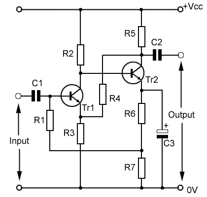
Fig. 3.2.6 DC coupled amplifier with negative feedback.
Negative feedback can create stability problems when the circuit contains capacitors in the signal or feedback paths. The problem can be reduced by using direct, instead of capacitive coupling. however, DC coupling normally requires extra feedback to maintain stable bias conditions.
The circuit in Fig. 3.2.6 shows a two stage directly coupled class A amplifier using voltage derived, series fed negative feedback and is an example of how the above problems may be overcome in a practical amplifier design.
The output signal at Tr2 collector is fed back to the emitter of Tr1 via the feedback network R4 R3. A portion β of the output signal equal to the ratio R3/(R4+R3) appears across the emitter, and assuming that R4 is 10KΩ and R3 is 1KΩ, β will be 1/11 and the closed loop amplification will be 1/β = 11.
Because the amplifier is DC coupled, the bias system also uses DC negative feedback with Tr1 base bias being derived from the emitter of Tr2. If the base voltage (VB) on Tr1 starts to increase for any reason, Tr1 collector voltage (VC) will fall and so will the directly coupled base of Tr2. This in turn will make the collector emitter current of Tr2 fall and so the voltage at the junction of R6 and R7 will also reduce. Since this point in the circuit is the supply point (via R1) for Tr1 base bias, the base voltage on Tr1 will also tend to fall, counteracting the original rise in base voltage and restoring the bias to the correct value. Any fall in Tr1 base voltage causing variations in the opposite sense to those described above will be counteracted in a similar manner.


