Module 6.1
Op Amp Inputs
- After studying this section, you should be able to:
- Recognise typical forms of op amp circuit symbols.
- Understand the need for single & dual power supplies.
- Understand typical operating requirements.
- • High gain & negative Feedback.
- • Differential inputs.
- • Constant current sourcing.
- • Common Mode Rejection, CMRR.
- • Offset null.

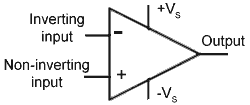
Fig. 6.1.1 Op Amp Circuit Symbol
Op Amp Circuit Symbol
The circuit symbol for an op amp is basically the standard triangle symbol for an amplifier. Main connections such as the inverting (−) and non-inverting inputs and the output are shown, but often, other connections are not. A typical op amp symbol is shown in Fig. 6.1.1. Note however, that many circuit diagrams do not show the DC supply connections.
Dual Power Supplies
An op amp needs a minimum of five connections as shown in Fig 6.1.1, as well as the two inputs and one output there are two power supply connections. These may be labelled +Vs and -Vs indicating that the IC needs both positive and negative supplies. These will often be in the range of +5V to +15V for the positive supply and -5V to -15V for the negative supply. This dual supply arrangement allows for the output voltage to swing both above and below zero volts, and also gives an output of 0V when there is no voltage difference between the two inputs.
Single Supply Op Amps
A growing number of op amps are available however, that use a single supply, labelled +V and Gnd or 0V. This is a useful arrangement for many portable and mobile applications where dual positive and negative supplies are not readily available, for example in automobile applications.
High Gain Negative Feedback DC Amplifier
Op amps are basically negative feedback (NFB) DC amplifiers. The op amp has a very large gain, the output can be hundreds of thousands times larger than the input. This huge gain however, is reduced using negative feedback to produce a circuit whose gain is stable and independent of the semiconductor characteristics.
Op amps are also always DC coupled, unlike an amplifier using discrete components where it is possible to include AC components such as capacitors and inductors, in a tiny integrated circuit it is not possible to fabricate AC components large enough to be useful at audio frequencies, therefore an op amp MUST be a DC amplifier.
One advantage of using DC (directly coupled or direct current) amplifiers is that their bandwidth extends right down to 0Hz, making them suitable for many control and measurement applications where the op amp’s ability to produce a DC output, relative to the difference between two DC input quantities is extremely valuable. The problem with directly coupled amplifiers however, is their tendency to drift, causing the DC voltages present in the circuit to change, especially with changes in temperature.
Because the op amp has a very high gain, it only takes a tiny change in voltage at the input to produce a large voltage change at the output. Because of this, op amp input circuits are designed around a differential amplifier, also called an emitter coupled amplifier or a long tailed pair, which provides the op amps two (inverting and non-inverting) inputs and also has the ability to cancel out voltage drift.
Difference Amplifier

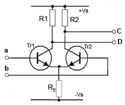
Fig.6.1.2 Emitter Coupled Amplifier
The Op amp’s basic operation is that of a difference amplifier, producing a voltage output that is proportional to the voltage difference at its two inputs. These inputs, labelled - (the inverting input) and + (the non-inverting input) form the inputs of an emitter coupled amplifier, a basic example of which is shown in Fig. 6.1.2, it consists of a pair of matched transistors Tr1 and Tr2, which share the same emitter resistor RE.
Suppose that one of the inputs (b) is held at a fixed voltage, proving a suitable base bias to make Tr2 conduct. If a signal is now applied to input (a), each time the signal voltage rises, Tr1 conduction increases, its collector voltage falls and its emitter voltage (the voltage across the shared RE) rises. This rise also causes a rise in the emitter voltage of Tr2, and as the base of Tr2 is fixed, the base-emitter voltage (VBE) of Tr2 decreases, and reduces the current through Tr2. This causes the voltage at Tr2 collector to rise, making the signal at output C rise in anti-phase to the output at D.
Provided that the transistors are ideally matched, and there are no other factors to cause differences between the conduction in each half of the circuit, the rise in current due to Tr1 conducting is cancelled out by the fall in current through Tr2, and the voltage across RE should not change. In practice the change would only be a few millivolts.
Common Mode Signals
If two identical signals are applied to each input, two possibilities may be considered:
1. The signals at each input are identical and in anti-phase with each other.
2. The signals at each input are identical and in phase with each other.
Condition 1 is called a differential input as there is a difference produced by the anti-phase signals. In this case the two amplified signals produced at the two outputs will be an amplified difference between the two signals, but as the output signals are in anti-phase with each other, as one signal voltage rises the other signal voltage falls and the resulting signal between outputs C and D will be twice the amplitude of either single output.
Condition 2 has both input signals in phase and so is called a common mode input. The outputs C and D are also in phase, both rising and falling together. Therefore the difference between outputs C and D is zero. The differential amplifier therefore can be said to amplify a differential input, but to reject, or to be immune to, a common mode input. This ideal rejection of common mode signals does not quite occur in practice as there are bound to be some slight differences between the gains between each of the two inputs and their respective outputs, even when, in an integrated circuit they are fabricated on the same piece of silicon. However, common mode signals that cause both Tr1 and Tr2 emitter currents to rise and fall in unison, will set up a changing voltage across the shared emitter resistor RE and because there is no decoupling across RE negative feedback will occur, causing the common mode gain of the amplifier to be reduced. This common mode feedback can be used to improve common mode rejection if a large value for RE is used.
Constant Current Source

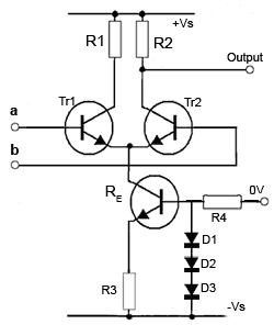
Fig.6.1.3 Constant Current Source
Rather than relying solely on the negative feedback produced by RE to improve common mode rejection in integrated circuits, most op amp ICs replace RE in the emitter coupled amplifier with a constant current source as shown in Fig. 6.1.3. This circuit is much more efficient at preventing variations in the shared emitter current of Tr1 and Tr2 that are due to common mode signals. The base of Tr3 is biased at relatively fixed voltage, in this case by a potential divider formed by R4 and the three forward biased diodes D1, D2 and D3, but other arrangements, usually consisting of some combination of diodes or zener diodes and resistors can be used.
In the presence of a common mode signal, the collector-emitter current through Tr3 will try to vary; any increase in this current would increase the voltage across R3, and any decrease would reduce it. However because the base voltage of Tr3 is held at a steady voltage, an increase in collector-emitter current will increase the emitter voltage and therefore reduce VBE. This will reduce the conduction of Tr3 and reduce the collector-emitter current, back to its original value. A decrease in Tr3 collector-emitter current would similarly increase VBE and increase conduction of Tr3 until the current is returned to normal once again. Including a constant current source in the emitter circuit of the differential amplifier makes the rejection of common mode signals very efficient.
Notice that in the circuit shown in Fig. 6.1.3 only a single output from Tr2 collector is used to produce a single amplified voltage that is proportional to the difference between inputs a and b, and is almost entirely unaffected by changes common to a and b. There are op amps available that use two outputs, but single output op amps are far more numerous.
Common Mode Rejection Ratio (CMRR)
Ideally the op amp output responds only to differential signals, but in practice, even when the inputs are at exactly the same potential, and the output should be at zero volts, some small output potential will be present. This is caused by inevitable small differences in gain between the inverting and the non-inverting inputs. The op amp therefore has some gain to common mode signals, which is indicated by the parameter Common Mode Voltage Gain (AVCM) and the ratio between this and the Differential Voltage Gain (AVD) is indicated in the main op amp parameters by the Common Mode Rejection Ratio CMRR. Because this ratio is normally a very large number it is often quoted in deciBels.
A reason that the CMRR is an important parameter is that when an op amp is used, as they often are, in circuits involving measurement, some error will be present, for example when measuring the difference between two very small voltages, this error is amplified along with the true differential voltage, so making any measurement inaccurate.
In some modes of operation common mode signals are not produced, for example when the op amp is used as an inverting amplifier, and the non-inverting input is grounded. Then the only time the inputs are the same is when they are both zero.
Offset Null

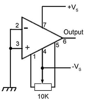
Fig.6.1.4 Offset Null Adjustment
If common mode signals are to be avoided, the gain from each of the inputs must match as closely as possible. To produce op amps with minimal common mode gain, manufacturers use various techniques such fabricating extra resistors to control the gain from each input within the chip, these may then be removed as required, by selectively blowing fuses to remove individual resistors from one or other channel to balance the input gains. Another, more accurate technique with tiny resistors embedded in the silicon chip, is to use lasers to trim the width of the resistors to alter their resistance during manufacture and testing process.
Although modern op amps can be made to have very low offset voltages many op amps provide two extra pins for additional external offset nulling. A typical offset null arrangement is shown in Fig. 6.1.4. A potentiometer is connected between the two offset null pins with the potentiometer wiper connected to the negative power supply. The inputs are both connected to ground and with power on and the IC running at ambient temperature the potentiometer is adjusted to make the output voltage = 0V. Note that it is quite common for the offset null potentiometer, although present in the actual circuit, to be omitted from the circuit schematic diagram, as once adjusted during manufacture it is not considered to play any further part in the circuit’s basic operation.
Because such small voltages are involved, the adjustment can be quite sensitive and where necessary the 10K potentiometer could be replaced by a 1K with 4K7 resistors fitted between each end of the potentiometer track and the offset null pins of the IC.


