Module 3.4
Wien Bridge Oscillators
- After Studying this section, you should be able to:
- Understand the operation of Wien Bridge Oscillators.
- • Lamp controlled circuits.
- • Diode controlled circuits.
- • AGC controlled circuits.
- Construct a lamp controlled Wien Bridge oscillator from given instructions.
Building Wien Bridge Oscillators with Modern Components
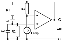
Fig. 3.4.1 Basic Lamp Stabilised
Wien Bridge Oscillator
The Wien Bridge oscillator can still be built using similar principles to the early Hewlett Packard versions, but with modern components.
Fig. 3.4.1 shows a basic Wien Bridge Oscillator using a filament lamp with an op amp. It is a property of filament lamps that the resistance of the tungsten filament increases in a non-linear manner as the filament heats up. The lamp in Fig. 3.4.1 is connected in the negative feedback potential divider that sets the gain of the non-inverting amplifier. The gain of the amplifier is set by:

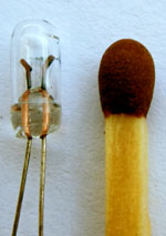
Fig. 3.4.2 Miniature Filament Lamp
Compared With a Match Head
Therefore the greater the resistance of the lamp the lower the amplifier gain. By choosing a suitable lamp, the gain of the amplifier can be automatically controlled over an appropriate range. Usually a lamp with a maximum current flow of around 50mA or less is used, to give an initial gain of more than 3 as the oscillator starts, falling quickly to 3 as the lamp heats up.
Hewlett’s original 1939 design used a high voltage vacuum tube (valve) and relatively large lamp, with modern low voltage semiconductors however, it is not easy to find suitable filament lamps that have a suitable voltage range and a low enough current to avoid overloading the amplifier, although useful lamps can still be found, usually of the wire ended T1 or ‘grain of rice’ types but even they are becoming more difficult to find in component suppliers catalogues, as LED types become more popular for low voltage lighting.
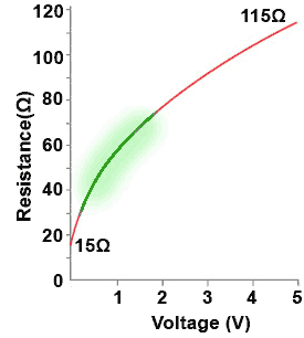
Fig. 3.4.3 Non-linear resistance
of a filament lamp
Fig. 3.4.2 shows a low current filament lamp designed to work from 5V at 45mA, and Fig. 3.4.3 is a graph taken from a typical example, showing how its positive temperature coefficient resistance varies with voltage. (Note that resistance without any temperature dependant characteristics would be a straight line). The useful area of the lamp characteristic, where the largest change in resistance occurs is shaded green, the oscillators amplitude is stabilised by making use of this area. However, because filament lamps are not made as electronic control devices, manufacturers do not usually provide graphs such as that in Fig.3.4.3 so, when using a lamp as a stabilising component it is necessary to first construct a graph for the lamp to be used, and decide on the active area.
The gain of the amplifier in Fig. 3.4.1 depends on the ratio of the values of the feedback resistor R3 and the lamp. For oscillations to start, the amplifier gain needs to be greater than 3, but to work correctly after the initial start up the gain must be 3. Using the formula:

This requires the lamp to be half the resistance of the feedback resistor R3 to provide the necessary gain of 3, but slightly less than twice the resistance of R3 at start up.
To find a value for R3 that will give the correct amount of gain at start up and during oscillation, its value should be slightly greater than twice the value of the lamps resistance at the lower end of the green shaded area (i.e. 2 x 30Ω = 60Ω) to give a gain >3, but no greater than twice the value of the lamp’s resistance at the upper limit of its useful slope (i.e. 2 x 75 = 150 Ω), the gain should then stabilise at 3, with the oscillator providing an undistorted sine wave output.
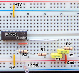
Fig. 3.4.4 Lamp Stabilised Circuit
on Breadboard
To obtain an undistorted output at a specific amplitude, it is useful to initially use a variable resistor of about 1kΩ in place of the feedback resistor. Varying the resistor will show the limits between the greatest amplitude before distortion and the smallest amplitude for stable operation. The resistance of the variable control can then be measured find the value of feedback resistor that provides a stable and undistorted wave of acceptable amplitude. In a test circuit, built using a LM324 op amp with a supply voltage of ±9V to ±12V a value of 68Ω to 82Ω proved ideal.
To find values for R and C in the Wien Bridge that will give a specific frequency:
The formula for frequency:

Can be re-arranged as:

and

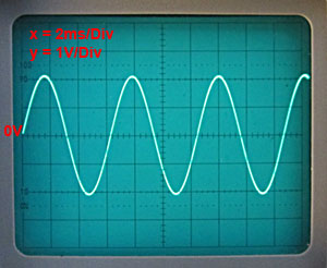
Fig. 3.4.5 Output Waveform from
Lamp Stabilised Circuit
These calculations will almost inevitably produce values that do not match available components so it will be necessary to choose a preferred value closest to the calculated one. It may be possible to make up an odd value from two preferred values to get closer to the required frequency, remembering that component tolerances will make absolute accuracy difficult to obtain. The test circuit shown in Fig. 3.4.4 used 10K and 100nF, which gives a calculated frequency of 159Hz, the measured frequency turned out to be 157Hz. The output wave of just over 4Vpp is shown in Fig 3.4.5. Because of the way the output stage of the LM324 is constructed, there can be a problem with crossover distortion when the op amp is operating in class B. In this demo circuit the distortion was so small that it can be ignored. It is present in the waveform shown in Fig. 3.4.5 but is obscured by the 0V line. For methods of removing more significant crossover distortion, see the circuits for the diode stabilised circuit and the AGC controlled circuit later in this module.
Construction on Breadboard
The circuit in Fig. 3.4.1 can be built on breadboard using Fig 3.4.4 as a guide, and calculating the values of C1, C2, R1 and R2 from the information above. Experiment with your own values, but for initial testing purposes, a list of components used in the circuit shown in Fig 3.4.4 is given below
Components List.
- IC1 = LM324
- C1 & C2 = 100nF
- R1 & R2= 10KΩ
- R3 = 68Ω
- Lamp = T1 5V 45mA wire ended lamp
- At the time of writing (2013) suitable lamps are available from Rapid Electronics UK)
Lamp Stabilised Wien Bridge Oscillator Measurements
Having built the Wien Bridge oscillator on breadboard check that the circuit is oscillating satisfactorily by displaying the output waveform on an oscilloscope.
1. Calculate the design frequency of the oscillator using:

_________________Hz
2. Using a multi-meter, take the DC measurements and complete Table A.
| Table A | |
|---|---|
| The +V supply | |
| The −V supply | |
3. Record the chosen value for the feedback resistor R3_______Ω

4. With an oscilloscope connected to the oscillator output, draw at least two cycles of the output waveform on the grid below. Enter the time/division and volts/division settings of the CRO in the spaces provided.
5. From the waveform, calculate and record the values in Table B.
| Table B | |
|---|---|
| Peak to Peak Output Voltage | |
| DC level of the wave | |
| Periodic time T of the wave | |
| Frequency of the wave (1/T) | |
Diode Stabilised Wien Bridge Oscillator
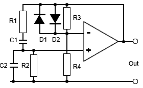
Fig. 3.4.6 Basic Diode Stabilised
Wien Bridge Oscillator
An alternative to lamp stabilisation is provided by using a pair of diodes in parallel with the feedback resistor as shown in Fig. 3.4.6.
In this circuit the gain of the non-inverting amplifier is controlled by the ratio of R3 to R4. Initially the gain set by R3 and R4 will be just slightly greater than 3, this will allow oscillations to start.
Once the signal fed back from the output produces a waveform across R3 that approaches 0.7Vpp the diodes will begin to conduct. Their forward resistance will reduce, and because they are in parallel with R3, this effectively reduces the value of R3 and so reduces the amplifier gain.
The main problem with this method is that the output wave can be more prone to distortion than in the lamp stabilised circuit as the diodes, which have a non-linear relationship between voltage and current, especially as they begin to conduct, will tend to distort the waveform peaks if the gain set by R3 and R4 is slightly higher than needed. This also means that the oscillator’s output amplitude is somewhat restricted if distortion is to be minimised.
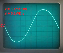
Fig. 3.4.7a Correct Gain Gives
Undistorted Output at 1.2Vpp
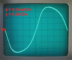
Fig. 3.4.7b With Output at only
1.35Vpp Output Starts to Distort
Fig. 3.4.7a shows that with the correct gain, producing an output of 1.2Vpp and the diodes just on the edge of conducting, the circuit provides an undistorted output, but with only a slight increase in output to 1.35Vpp the diodes start to conduct more heavily and distortion is already becoming apparent. Careful examination of Fig. 3.4.7b shows the peaks of the sine wave are just beginning to be asymmetrical, with the rising slope of the wave steeper than the falling slope. Any further increase in gain would cause greater distortion.
Variable Frequency Wien Bridge
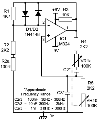
Fig. 3.4.8 Diode Stabilised Variable
Frequency Wien Bridge Oscillator
Fig. 3.4.8 shows a practical diode stabilised circuit with variable frequency that can be built on breadboard to learn by experiment.
The range of frequencies may be extended using different capacitor values for C2 and C3 as indicated in the diagram. The gain of the amplifier is set by the ratio of R1 to R2 and R2a at 3.04. If R2a is omitted the gain increases to 3.136, which still gives an output but with slightly increased distortion as shown in Fig. 3.4.7b.
An interesting experiment is to replace R2/R2a by a variable resistor (4k7) and see the margin between distortion (too much gain) and failure to oscillate (too little gain) by slightly changing the gain.
The values of the gain setting components in Fig. 3.4.8 are carefully chosen to give a gain just greater than 3. It is the ratio of the component values rather than the values themselves that govern the amount of gain. What is the effect if R1, R2 and R2a are replaced by 47K, 22K and 1K respectively?
Potentiometer problems
Some problems crop up when using real components on breadboard that do not readily show up in computer simulations. These include a particular problem when using variable resistors in Wien Bridge oscillators.
Fig. 3.4.9 Testing Potentiometer Tracking
Ideally both resistors in a dual potentiometer would have identical resistance values. Small differences are normally not noticeable when using these potentiometers in stereo audio systems for example, but unless a considerable amount is spent on buying special potentiometers that not only have matched resistances but also both change resistance by exactly the same amount as the wiper contacts of the resistors move, quite small mismatches can cause problems in circuits such as the Wien Bridge.
The resistance from the wiper to either end of the resistance track should be identical on both controls for any angle of rotation of the control. The effect of inaccurate tracking is that at some angles of rotation, the slected resistances of VR1a and VR1b may not be equal, causing the balance of the bridge circuit to be upset, then the amplitude of oscillation may vary, or oscillations may even cease altogether. A simple method of testing the tracking ability of a dual potentiometer is shown in Fig 3.4.9.
Both potentiometers are connected across a low voltage supply, (low enough voltage to avoid excessive current through the control), and a voltmeter connected between the two sliders. As the control is adjusted over its full range, the voltage on both sliders should be the same and so the voltmeter will always read zero volts. It is most likely that with standard potentiometers the reading will not remain at zero but the test can help in choosing the most suitable dual control.
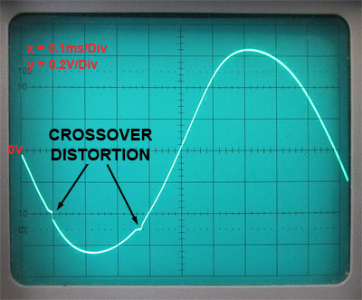
Fig. 3.4.10 Crossover Distortion in the LM324 Output
Crossover Distortion
The circuit suggested in Fig. 3.4.8 uses one section of a LM324 quad op amp, which has an output that works in class A but changes to class B with large signals. This can make it susceptible to crossover distortion. The recommended way to eliminate this is to force the output to work in single ended class A mode by connecting an external resistor between the output and either ground or supply. In this circuit a 10K resistor (R3 in Fig. 3.4.8) to supply eliminates crossover distortion. For different signal and supply levels the value of R3 may need to be varied, again - experiment.
Wien Bridge Oscillator with AGC
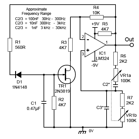
Fig. 3.4.11 Wien Bridge Oscillator with AGC
A JFET can be used to provide automatic gain control (AGC) as shown in Fig 3.4.11. This can provide a larger amplitude output and less distortion than the diode version shown in Fig. 3.4.8, and unlike the lamp stabilised version, uses readily available components.
This circuit has a variable frequency using a dual ganged potentiometer arrangement similar to the diode stabilised circuit, with R6 and R7 reducing the load on the amplifier output if the bridge potentiometers are adjusted to zero ohms. R5 is added to prevent crossover distortion problems.
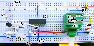
Fig. 3.4.12 AGC Wien Bridge Oscillator on Breadboard
Fig. 3.4.12 shows an experimental Wien Bridge AGC oscillator built on breadboard. It has useful frequency ranges depending on the capacitors used, as shown on the circuit diagram in Fig. 3.4.11 although the output can be found to reduce in amplitude and exhibit distortion at the extreme upper frequencies (above the range indicated) in each range, due to the loading of the output by the low resistances of the potentiometers. Fitting higher value resistors for R6 and R7 reduces this effect but also restricts the frequency range.
Fig. 3.4.13 illustrates a typical sine wave output of 17Vpp at 1kHz, a considerably larger amplitude than is possible with the diode stabilised circuit in Fig. 3.4.8. The wave shape is quite good, though careful examiation will reveal a very slight difference in the shape of the two half cycles, the negative half cycle being slightly more pointed than the positive half cycle.
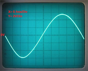
Fig. 3.4.13 AGC Wien Bridge Output at 1kHz
Automatic Gain Control (AGC)
Fig. 3.4.14 shows a computer simulation of the oscillator waveforms during the first 45ms after start up, and how the AGC system stabilises the amplitude of the output wave. The output wave of IC1 is coloured green and the input signal is shown by the blue waveform. The controlling voltage applied to the gate of TR1 is coloured red. The numbers in circles refer to the numbered paragraphs below.
The gain of the amplifier is initially set by the ratio of R4(10K) and R3(4K7)

1. For the first few milliseconds after switch on, the voltage on TR1 gate is 0V, therefore the drain/source channel has a very low resistance compared with R3 and the gain of the amplifier is 3.13, and after 5ms the output waveform begins to grow rapidly.
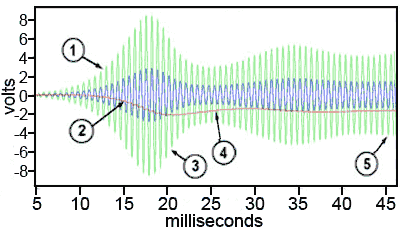
Fig. 3.4.14 AGC Action at Start-up
2. The output wave is fed back to D1, which rectifies the negative half cycles of the wave to produce a negative DC voltage that grows negatively as C1 charges.
3. As TR1 gate becomes more negative, the resistance of the JFET increases, adding to the resistance of R3 and reducing the amplifier gain.
4. The output amplitude falls too far, slightly over compensating, but this reduces the negative gate voltage allowing the output to increase again.
5. After about 45ms the gate voltage VGS settles at about –2V and the system stabilises the gain at 3 and the input wave can now be seen to be 1/3 of the amplitude of the output wave.


