Module 3.1
Buck Converters

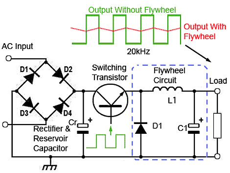
Fig. 3.1.1 The Buck Converter
- After studying this section, you should be able to:
- Understand the principles of Buck Converters.
- • The Switching Transistor.
- • The Flywheel Circuit.
- Recognise the limitations on the output voltage.
- Recognise different input sources.
- Understand the relationship between switching pulse width and output voltage.
The Buck Converter
The Buck Converter is used in SMPS circuits where the DC output voltage needs to be lower than the DC input voltage. The DC input can be derived from rectified AC or from any DC supply. It is useful where electrical isolation is not needed between the switching circuit and the output, but where the input is from a rectified AC source, isolation between the AC source and the rectifier could be provided by a mains isolating transformer.
The switching transistor between the input and output of the Buck Converter continually switches on and off at high frequency. To maintain a continuous output, the circuit uses the energy stored in the inductor L, during the on periods of the switching transistor, to continue supplying the load during the off periods. The circuit operation depends on what is sometimes also called a Flywheel Circuit. This is because the circuit acts rather like a mechanical flywheel that, given regularly spaced pulses of energy keeps spinning smoothly (outputting energy) at a steady rate.
AC or DC Input
The buck converter is a form of DC to DC converter that can take an input directly from a DC source, such as a battery. The input could also be DC derived from the AC mains (line) as shown in Fig. 3.1.1 via a rectifier/reservoir capacitor circuit. The AC input to the rectifier circuit could be AC at high voltage directly from the AC mains supply, or alternatively at a lower voltage via a step down transformer. However the DC applied to the Buck Converter is obtained, it is then converted to a high frequency AC, using a switching or ‘chopper’ transistor, driven by a (usually pulse width modulated) square wave. This results in a high frequency AC wave, which can then be re-converted to DC in a much more efficient manner than would be possible in the circuits described in Power Supplies Module 1.
Buck Converter Operation

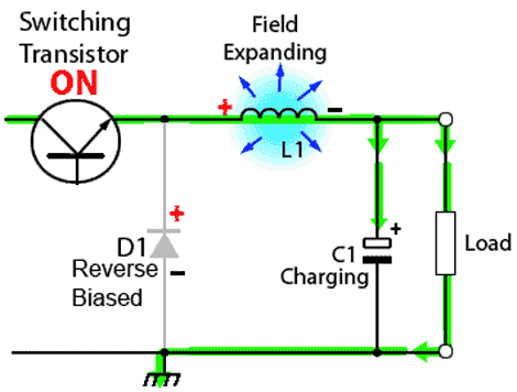
Fig. 3.1.2 Switching Transistor ‘on’ Period
As shown in Fig. 3.1.1 the buck Converter circuit consists of the switching transistor, together with the flywheel circuit (Dl, L1 and C1). While the transistor is on, current is flowing through the load via the inductor L1. The action of any inductor opposes changes in current flow and also acts as a store of energy. In this case the switching transistor output is prevented from increasing immediately to its peak value as the inductor stores energy taken from the increasing output; this stored energy is later released back into the circuit as a back e.m.f. as current from the switching transistor is rapidly switched off.
Transistor Switch ‘on’ Period
In Fig. 3.1.2 therefore, when the switching transistor is switched on, it is supplying the load with current. Initially current flow to the load is restricted as energy is also being stored in L1, therefore the current in the load and the charge on C1 builds up gradually during the ‘on’ period. Notice that throughout the on period, there will be a large positive voltage on D1 cathode and so the diode will be reverse biased and therefore play no part in the action.

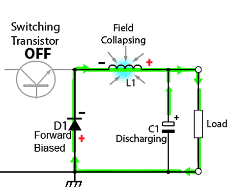
Fig. 3.1.3 Switching Transistor ‘off’ Period
Transistor Switch ‘off’ Period
When the transistor switches off as shown in Fig 3.1.3 the energy stored in the magnetic field around L1 is released back into the circuit. The voltage across the inductor (the back e.m.f.) is now in reverse polarity to the voltage across L1 during the ‘on’ period, and sufficient stored energy is available in the collapsing magnetic field to keep current flowing for at least part of the time the transistor switch is open.
The back e.m.f. from L1 now causes current to flow around the circuit via the load and D1, which is now forward biased. Once the inductor has returned a large part of its stored energy to the circuit and the load voltage begins to fall, the charge stored in C1 becomes the main source of current, keeping current flowing through the load until the next ‘on’ period begins.
The overall effect of this is that, instead of a large square wave appearing across the load, there remains only a ripple waveform, i.e. a small amplitude, high frequency triangular wave with a DC level of:
VOUT = VIN x (On time of switching waveform (tON) / periodic time of switching waveform( T))
or:

Fig. 3.1.4 Buck Converter Operation
Therefore if the switching waveform has a mark to space ratio of 1:1, the output VOUT from the buck Converter circuit will be VIN x(0.5/1) or half of VIN. However if the mark to space ratio of the switching waveform is varied, any output voltage between approximately 0V and VIN is possible.
Buck Converter Operation Video
See the current paths during the on and off periods of the switching transistor.
See the magnetic field around the inductor grow and collapse, and observe the changing polarity of the voltage across L.
Watch the effect of ripple during the on and off states of the switching transistor.
Note that the actions illustrated in Fig. 3.1.4 are greatly slowed down; the transitor would normally be switching on and off at 20KHz or faster.
Buck Converter for Negative Supplies

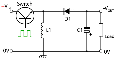
Fig. 3.1.5 Buck Converter for Negative Supplies
In many complex circuits, the main DC supply may be at a too high voltage for some parts of the circuit. E.g. a 24Vdc supply for an output stage may need to be reuduced to 5V or 3.3V for logic circuits driving the output stage. In some circuits it may also be necessary to cater for negative supplies. For such circumstances the circuit shown in Fig. 3.1.5 can be used. This involves a change around in the positions of L1 and D1, and reversing the polarity of C compared to the circuit in Fig 3.1.2. This variation of the basic buck converter now inverts the positive DC input to produce a negative supply in the range of 0V to −VIN.
How Fig. 3.1.5 Works
When the transistor switch turns on the positive supply voltage is applied to L1. The diode D1 is reverse biased at this moment, so the supply current cannot reach the output, but charges L1, creating a magnetic field to build up around it. Notice that the voltage across L1 at this time causes the top of the inductor to be positive with respect to the 0V line.
When the input transistor switches off however, the magnetic field around L1 begins to collapse, and so induces a reversal of voltage across L1 that now makes the top of L1 negative with respect to 0V. At this time D1 becomes forward biased and conducts, causing the capacitor C1 to chare up producing a negative output voltage across the load. The actual value of negative output voltage will be the inverse of some fraction of the input voltage and depends on the mark to space ratio of the square wave signal applied input switch, which will be a pulse width modulated signal, typically operating at a constant frequency at tens of KHz.


