
Google Ads
Module 2.4
Zener Diodes
- After studying this section, you should be able to:
- • Describe typical Zener Diode construction.
- • Describe the Zener effect.
- • Describe the Avalanche effect in Zener Diodes.
- • Describe typical Applications for Zener Diodes.
- • Shunt voltage regulation.
- • Series voltage regulation.
- • Calculate appropriate values for current limiting resistors for Zener Diodes.
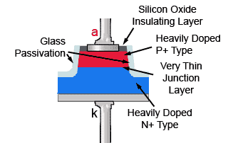
Figure 2.4.1. Zener Diode Construction
Zener Diode Construction
Zener diodes are a modified form of PN silicon diode used extensively for voltage regulation. The P type and N type silicon used is doped more heavily than a standard PN diode. As shown in Fig. 2.4.1, this results in a relatively thin junction layer, and consequently a reverse breakdown voltage that can be much lower than in a conventional diode. The actual breakdown voltage is controlled during manufacture by adjusting the amount of doping used. Breakdown voltages can be selected in this way to occur at precise preset values anywhere between about 3V and 300V. Zener diodes can also withstand higher reverse current flow than comparable PN diodes, and are available with various power ratings, typically from 500mW to 50W.
When Zener diodes are biased in their forward direction, with the anode voltage higher than the cathode, they behave in the same way as a normal silicon diode. When they are reverse biased they exhibit a very high resistance, and consequently a low value of reverse leakage current. However when a reverse bias reaches the value of the diode´s reverse breakdown voltage (the Zener voltage) a rapid drop in resistance and increase in current occurs. To prevent this current increasing to a value that would exceed the diode´s power rating and destroy it, the Zener diode uses a resistor connected in series with the diode to limit the reverse current to a safe value.
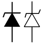
Figure 2.4.2. Alternative
Zener Diode Symbols
Operating the diode in this condition means that, due to the very steep slope of the diode´s reverse characteristic, any slight change in voltage across the diode will cause a large change in current through the diode. This effect is very useful in voltage regulator circuits, as explained in our Power Supplies Modules 2.1(Shunt Voltage Regulators) and 2.2 (Series Voltage Regulators). Zener diodes are also useful for providing an accurate reference voltage for purposes such as waveform clamping. This rapid increase in reverse current in Zener diode operation is due to one or both of two effects:
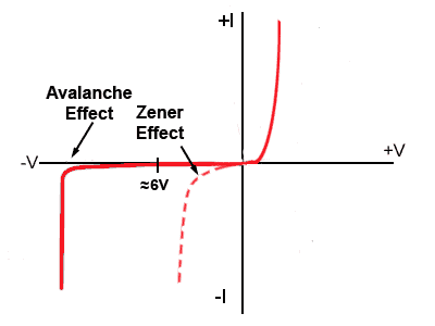
Figure 2.4.3. Zener & Avalanche Effects
1. The Zener Effect
Because of the heavily doped P and N materials at either side of the junction, which are therefore good conductors, and the very thin depletion layer, the electric field strength across the depletion layer is very strong, and it becomes relatively easy, even at low voltages, for holes and electrons to cross the depletion layer and combine to create a reverse current. This effect mostly happens in Zener diodes with a low reverse breakdown voltage, typically 5 to 6V or less and leads to a gradual, rather than a sudden increase in reverse current.
2. The Avalanche Effect
In Zener diodes with wider depletion layers and therefore higher breakdown voltages, the increase in current at the breakdown voltage is much more sudden, giving an abrupt reduction in the reverse resistance of the diode and a nearly vertical region to the diode´s reverse current characteristic. This effect happens mainly in diodes with a higher reverse breakdown voltage (above about 5V) and less heavily doped P and N regions. Below the reverse breakdown voltage, although only a small reverse leakage current is flowing, some current does flow and therefore electrons and holes are entering the depletion layer. As the reverse voltage approaches the reverse breakdown voltage the electrons and holes entering the depletion layer come under the effect of a strong electric field and are rapidly accelerated. In this accelerated state they begin to collide with other atoms and knock electrons from their atomic bonds in a process called ‘impact ionisation’, so creating more electron/hole pairs that are also greatly accelerated by the electric field. These secondary current carriers in turn ionise other atoms, creating a very rapid increase in reverse current through the diode. This process is called ‘Avalanche Breakdown’
Practical Zener Diodes
Practical zener diodes may use either the zener effect or the avalanche effect and in some diodes both effects can also occur at the same time, but it is common practice to call all these diodes zener diodes. Both the zener and avalanche effects are also dependant to some degree on the junction temperature of the diode. However, whist the current in a purely zener diode has a negative temperature coefficient i.e. the current reduces with an increase in temperature, the opposite effect occurs in a diode using the avalanche effect. Therefore it is possible to manufacture zener diodes that use both effects and so these temperature effects tend to cancel each other out, producing diodes that have very minimal current variation due to temperature.
Zener diodes are widely used in power supply circuits for both voltage regulation and over voltage protection, how they are used is discussed in much more detail in our Power Supplies Module 2.1.