
Google Ads
Module 2.7
Photodiodes
- After studying this section, you should be able to:
- Describe Different methods of photodiode operation:
- • Photovoltaic.
- • Photoconductive.
- Describe the basic construction of photodiodes.
- Describe the operation of different types of photodiode:
- • Photoconductive diodes.
- • PIN Photodiodes.
- • Avalanche Photodiodes.
- Describe typical limitations in photodiode operation.
- • Dark current.
- • Noise.
- Describe the reason for the choice of common materials used in photodiode construction.
- • Silicon.
- • Germanium.
- • Gallium Arsenide.
- • Indium Gallium Arsenide.
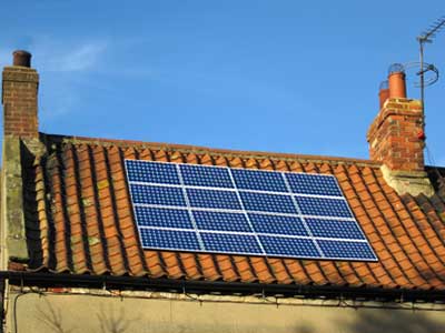
Fig. 2.7.1 Photovoltaic Diodes
(Solar Panels)
Photodiode Basics
Photodiodes basically perform the opposite effect to LEDs and laser diodes. Instead of using electric current to cause electrons and holes to combine to create photons, photodiodes absorb light energy (photons) to generate electron-hole pairs, so creating an electric current flow.
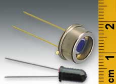
Fig. 2.7.2 Typical
Photoconductive Diodes
Photodiode Families
Two basic methods for generating electricity from light, using photodiodes are photovoltaic and photoconductive operation. Both methods use light sensitive semiconductor diodes, the chief difference is that photovoltaic devices, mainly used in solar panels (Fig. 2.7.1) do not use any bias voltage applied to the diode, but in photoconductive operation (Fig. 2.7.2) photodiodes have a reverse bias voltage applied from some external source.
Photodiode Applications
Photoconductive diodes are used in electronic systems such as fibre optic communications (this text has been delivered to you using photodiodes). Cameras use photodiodes to measure light, and to control the shutter, focus and flash. Medical uses include X-ray detection and pulse measurement. Photoconductive diodes are the sensor of choice for many industrial systems where light needs to be measured, from bar code scanners and position sensors to smoke detectors and surveying instruments. In applications involving high frequency changes in light levels, such as fibre optic communications it is important to keep the junction capacitance of the diode to a minimum, as quite a small capacitance would remove the higher frequencies and seriously reduce the efficiency of the photodiode receiver. Photoconductive diodes are therefore manufactured in small physical sizes, which generate very small amounts of electric current. Photovoltaic diodes by contrast are manufactured as very large size solar panels to maximise the efficiency of light collection. Solar panels necessarily have a much larger junction capacitance than photoconductive devices, but their efficiency is not reduced as they are designed to produce (much greater) electric current at DC (0Hz).
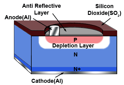
Fig. 2.7.3 Basic Photodiode Construction
Photodiode Construction
The typical construction of a photodiode is illustrated in Fig. 2.7.3. This example uses a construction technique called ion implantation where the surface of a layer of N type is bombarded with P type silicon ions to produce a P type layer about 1 µm (micrometre) thick. During the formation of the diode, electrons from the N type layer are attracted into the P type material and holes from the P type are attracted into the N type layer, resulting in the removal of free charge carriers close to the PN junction, so creating a depletion layer (shown in white in Fig. 2.7.3).
The (light facing) top of the diode is protected by a layer of Silicon Dioxide (SO2) in which there is a window for light to shine on the semiconductor. This window is coated with a thin anti-reflective layer of Silicon Nitride (SiN) to allow maximum absorption of light and an anode connection of aluminium (Al) is provided to the P type layer. Beneath the N type layer is a more heavily doped N+ layer to provide a low resistance connection to the cathode.
Photodiode Operation
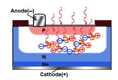
Fig. 2.7.4 Photons Create Electron/Hole Pairs
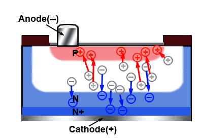
Fig. 2.7.5 Holes and Electrons are Attracted
by Reverse Bias
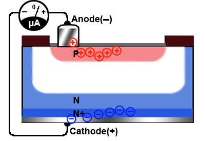
Fig. 2.7.6 Holes and Electrons Form
a Photoelectric Current
For a diode operating in Photoconductive Mode, it is usual to use reverse bias by applying a DC voltage to make the cathode more positive than the anode. This has the effect of widening the depletion layer as shown in Figs. 2.7.4 and 2.7.5.
Because the P and N layers with the depletion layer between them effectively form a capacitor, widening the depletion layer reduces the capacitance of the PN junction and increases the maximum frequency at which the diode can operate; a desirable property, especially in photodiodes that operate as digital information receivers.
When the surface of the photodiode is illuminated, as shown in Fig. 2.7.4 photons are absorbed within the diode and, mainly in the depletion layer, energise negative electrons in the valence layer of atoms, to jump to the higher energy level in the atom´s conduction band.
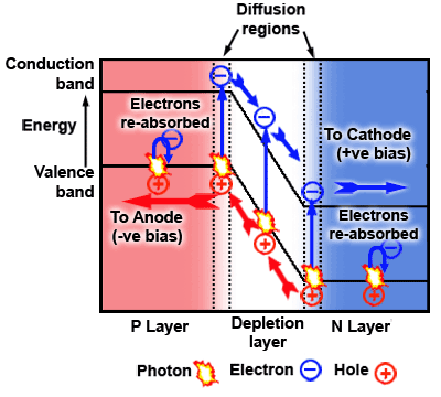
Fig. 2.7.7 Energy Band Diagram
of Photodiode Action
This leaves positively charged holes in the valence band, so producing ‘electron/hole pairs’ in the depletion layer. Some electron hole pairs are also produced in the P and N layers, but apart from those produced in the diffusion region N layers, most will be re-absorbed within the P and N materials as heat. The electrons in the depletion layer are then swept towards the positive potential on the cathode, and the holes swept towards the negative potential on the anode, so creating a photo current, as shown in Fig. 2.7.6.
Although Figs. 2.7.4 to 2.7.6 show different stages in the conversion of light energy into electric current, it should be realised that these steps all take place simultaneously and as a continuous process as long as the receiving surface of the photodiode is illuminated. An alternative way of illustrating photodiode action is to use an energy diagram, as shown in Fig. 2.7.7. This plots the energy levels of the valence and conduction bands of the (silicon) atom on the vertical axis of the diagram, against the distance between the anode and cathode of the photodiode on the horizontal axis.
In Fig.2.7.7 photons striking atoms within the depletion layer and the diffusion regions of the P and N layers are illustrated as little flashes of energy, each of which excites an electron to jump (vertical blue arrows) to the higher energy level conduction band. Note that electron/hole pairs created within the body of the P and N layers are re-absorbed as heat. Once the electrons and holes are separated, the reverse bias applied to the anode and cathode of the diode takes over, sweeping electrons towards the (positive) cathode and holes towards the (negative) anode, (large blue and red arrows).
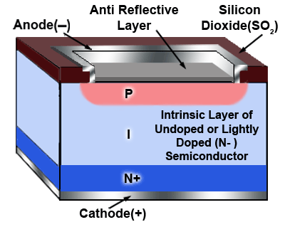
Fig. 2.7.8 PIN Photodiode
Reducing Junction Capacitance
The PIN Photodiode
This photodiode uses a layer of intrinsic (un doped or sometimes lightly doped N−) semiconductor between the P and N layers, see Fig. 2.7.8. This has the effect of reducing the capacitance of the PN junction and therefore improving the maximum switching speed, especially suited for fibre optic communications. The comparatively deep intrinsic layer also provides a larger volume for photon to electron/hole conversion.
PIN photodiodes are used in the Photoconductive Mode with a reverse bias applied, the relationship between the amount of light received and electric current produced is practically linear and they are also relatively stable over their normal temperature range.
Dark Current and Noise
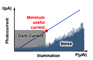
Fig. 2.7.9 Dark Current and Noise
The current produced by the photodiode process is extremely small, in the region of nano amps (nA) to a few micro amps (µA), and although the relationship between the amount of light shining on the photodiode and the current produced is quite linear, under very low light conditions the photo current produced is masked by the normal reverse leakage current due to thermal activity within the atomic structure of the diode. This current is referred to as ‘dark current’ as it is still present when the diode is not illuminated.
The small value of photoelectric current produced by the photodiode, and the presence of the thermally produced dark current, results in the photodiode´s useful range being significantly limited at low light levels.
Due to the extremely low signal levels obtainable from photodiodes, thermally produced noise is also a problem, especially where photodiodes may be used to detect low light levels. The ‘Minimum Useful Current’ for light detection is the photo current that is equal to the dark current plus the thermally produced noise generated by the diode as shown in Fig. 2.7.9.
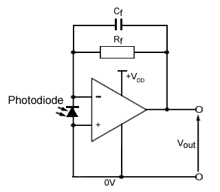
Fig. 2.7.10 Transimpedance Photodiode Amplifier
Generally the very small signal current from the photodiode will be amplified in some way, Fig 2.7.10 illustrates a typical amplifier circuit using a Transimpedance Op-amp. This amplifier has a low input impedance and translates the small current variations at its input into much larger voltage variations at its output. The amplifier gain is set by the value of Rf, and Cf helps to avoid instability. However it is also useful to create the largest signal current amplitude possible within the photodiode before it is amplified by an external circuit. As any electronic amplifier will also introduce some noise, one answer to this is to use the photodiode itself to produce a useful degree of amplification; this is the purpose of the Avalanche Photodiode.
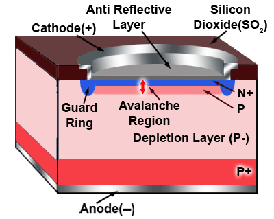
Fig. 2.7.11 Avalanche Photodiode
Avalanche Photodiodes
The purpose of the avalanche photodiode is to provide an initial amplification of photo current within the diode itself. It does so by operating with a much larger reverse bias than other photodiodes. This can mean that the diode is operating close to the reverse breakdown area of its characteristics. Fig. 2.7.11 shows one typical structure of an avalanche photodiode. Notice that the P+ anode is made negative and the N+ cathode layer is positive to provide the reverse bias.
Using such a high voltage reverse bias (typically 20V or more) provides a wide depletion layer, which forms a large collection area where photons create electron/hole pairs. This high voltage across the depletion layer also creates a strong electric force field that accelerates the electrons towards the positive potential on the cathode (and the holes towards the anode).
Amplification by Impact Ionisation
Notice particularly the doping used for the various layers of the photodiode. The N + layer immediately beneath the anti-reflective layer is heavily doped. Beneath this is a normally doped P layer, forming the PN junction of the diode; the main body of the diode is a lightly doped P− layer with a heavily doped P+ layer next to the anode connection.
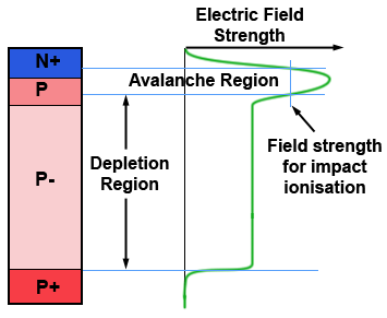
Fig. 2.7.12 Impact Ionisation
The level of doping in a semiconductor affects its resistance, the more heavily doped layers having the lowest resistance. For a particular value of current flow through the diode layers, which are effectively a series of different value resistances, causes different voltage values across the different layers. This creates an uneven electric force field across the diode as illustrated in Fig. 2.7.12.
The greater the electric field strength, the more acceleration is given to the electrons in the semiconductor. At the bottom of the diagram (Fig. 2.7.9) the heavily doped P+ layer next to the diode anode has a low resistance to aid efficient coupling to the metal anode connector. In the depletion region the resistance of the P− semiconductor is higher, providing sufficient field strength to accelerate the electron/hole pairs created by the photons. It is necessary, because of the depth of this area to move the charge carriers (electrons and holes) as quickly as possible to give the photodiode a fast response to changes in light level.
As electrons are attracted into the avalanche region around the more heavily doped P N+ junction, the higher resistance of these layers creates a higher voltage and so a higher field strength, which accelerates the electrons even further. When these highly accelerated electrons impact valence electrons in the atoms of the semiconductor material, they cause these previously bound valence electrons to jump into the conduction band, creating extra charge carriers. These new charge carriers (electrons) now also have sufficient energy to dislodge more electrons by impact and so on, creating an avalanche of extra electrons, which of course creates extra current.
By this method, called Impact Ionisation, the original very small current created by photons has effectively been amplified. The amount of amplification depends on the accelerating voltage, which may range between about 20V to several hundred volts. Additional factors affecting the amplification are the thickness of the avalanche region and number of electrons taking part in the impact ionisation process.
Because the number of impacts is random, the amount of amplification over any short period of time will vary, and so can only be quoted as an average value. Also because of the random nature of the photon impact, the output current will tend to be noisy due to the rapid fluctuations in amplification.
Avalanche photodiodes do not have as good a linear relationship between the light received and current produced as the other photoconductive diodes already described, but that is not necessarily a serious drawback in their main application, which is as a receiver of digital information in fibre optic communications and other high speed switching applications.
Photodiode Materials
Photodiodes use various semiconductor materials in their construction, chiefly to allow manufacturers to make a range of photodiodes that respond to different parts of the visible spectrum, as well as ultra violet and infra red wavelengths. Fig 2.7.13 shows the approximate wavelengths covered by some common semiconductor materials used for photodiodes.
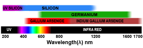
Fig. 2.7.13 Approximate Wavelength Ranges of Common Photodiode Materials
Silicon Photodiodes
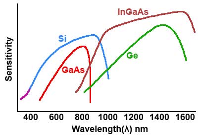
Fig.2.7.14 Relative Sensitivity of
Photodiode Semiconductors
Silicon (Si) photodiodes are popular for optical data receivers as they can be manufactured with a low value of junction capacitance, making them suitable for receiving digital data with frequencies up to several GigaHertz. They also generate relatively low amounts of dark current noise. However they also have a worse photon absorption rate than some other materials, which reduces their sensitivity.
Although silicon can be used over a wide range of wavelengths, from ultra violet (using specially designed UV versions) to the infra red wavelengths, silicon photodiodes are most useful in the 800 to 900nm range, as shown in Fig.2.7.14.
Germanium Photodiodes
Although Germanium (Ge) has been superseded in many diode applications it is useful in photodiodes as it provides light sensitivity at wavelengths longer than 900nm where Silicon is less sensitive, and Germanium is less expensive than Indium Gallium Arsenide (InGaAs), which makes it useful in photodiodes with large detection areas (up to around 1cm diameter). However Germanium photodiodes generally have higher levels of dark current and create comparatively more noise than either Silicon or Indium Gallium Arsenide, the noise level also increases at higher temperatures.
Indium Gallium Arsenide Photodiodes
Photodiodes using Indium Gallium Arsenide provide extra sensitivity in low light conditions especially at wavelengths in the infra red regions compared with either Silicon or Germanium. They generate less than half the noise and are more stable over a wide temperature range than Germanium.