Module 4.2
Op-amp Astables
- After studying this section, you should be able to:
- • Understand the operation of astable oscillators using op-amps.
- • Describe the limitations due to Slew Rate.
- • Calculate the frequency of an op-amp astable.
- • Describe methods for changing the frequency and mark to space ratio of op-amp astables.
How Op Amp Astables Work
Astables can be constructed around op amps and may use fewer components than the BJT designs described in Oscillators Module 4.1. Op amp designs are very useful, especially at low frequencies; at higher frequencies however, unless high speed op amps are used a problem occurs, as many standard (and older design) op amps are not able to handle the very fast voltage transitions required for good square wave shape, due to slew rate limiting.
The slew rate of an op amp is measured in V/μs (Volts per microsecond), and the output voltage of an astable must be able to change very rapidly by almost the full amount of the supply voltage as the output switches from low to high or back to its low level. However, a typical slew rate for many popular op amps may be around 0.5V/μs and such an op-amp would therefore would take 36μs for the output voltage to change by the 18V between –9V to +9v on a standard dual supply.
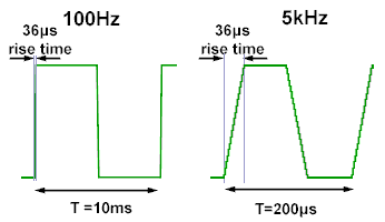
Fig. 4.2.1 The Effect of Slew Rate on Square Waves
Fig. 4.2.1 shows this may not be a problem in a low frequency astable; for example the 36μs rising edges and falling edge would occupy 72μs, just 0.72% of the 10ms periodic time of a 100Hz square wave. However in a 5kHz square wave, having a periodic time of only 200μs the slopes of the rising and falling edges would occupy 36% of the whole cycle of the wave.
Reducing the supply voltage would help overcome this problem to some extent, but a better solution is to use a high-speed op amp, which will have slew rate in excess of 10V/μs. A number of op amps fit this specification and some may also operate from a single power supply of 3V or less. Using comparators, which have a much faster response time (the term ‘slew-rate’ is not really applicable to comparators) than standard op-amps is also a good option for higher frequency designs.
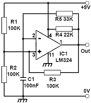
Fig. 4.2.2 Basic Op-amp Astable
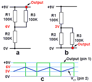
Fig. 4.2.3 Astable Circuit Operation
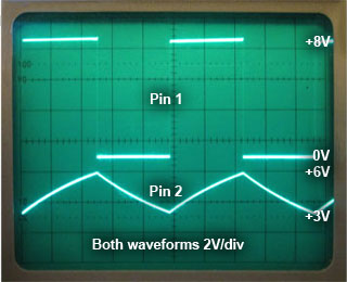
Fig. 4.2.4 Astable Circuit Waveforms
Fig. 4.2.2 shows a basic astable circuit using a LM324 operating from a single +9V supply, and suitable for generating square wave or pulse signals up to a frequency of about 2kHz. The operation of the circuit relies on repeatedly charging and discharging C1 from the output of the op amp via R5; these two components therefore set the operating frequency of the oscillator.
R1, R2 and R3 control the maximum and minimum voltage that C1 charge attains during a cycle of oscillation, and the purpose of R4 is to force the class B output of the LM324 into class A to avoid any crossover distortion in the output waveform as described in Oscillators Module 3.4.
Astable Circuit Operation
Assuming the output (pin 1 of IC1) of the LM324 in Fig. 4.2.2 is at the supply voltage of (+9V), R1, R2 and R3 can be considered to be connected as shown in Fig. 4.2.3a where R1 and R3 are connected in parallel and therefore have an effective resistance of:
100KΩ/2 = 50KΩ
As this parallel resistance of 50KΩ forms a potential divider with R2(100KΩ) and with a supply of +9V the voltage at the centre point of the divider will be 2/3 of 9V = 6V. While the output is high C1 will be charging at a rate determined by R5 towards +9V.
Once the capacitor (also connected to pin 2 of IC1) reaches a voltage of 6V however, it will exceed the voltage on pin 3, and the amplifier, due to its high gain, will act as a comparator and its output will immediately change to 0V.
The output end of R3 is therefore now connected to 0V creating the condition illustrated in Fig. 4.2.3b. The potential on pin 2 of IC1 is now 3V and the capacitor will be discharging via R5 towards the new output potential of 0V. On discharging past 3V however, pin 2 of IC1 becomes less than pin 3 and the amplifier output returns to +9V, completing one whole cycle.
The action repeats, generating a square wave at pin 1 of about 8Vpp and a 3Vpp triangular wave at pin 2 of the op amp. The actual waveforms produced by this circuit are shown in Fig. 4.2.4.
With the component values shown in Fig. 4.2.2 the circuit oscillates at a frequency slightly above 200Hz. The formula relating the frequency of oscillation, to the values of R5 and C1, allowing for the partial charge and discharge of C1 is therefore:

or

Note: The natural log (ln) of 2 is often shown as 1.4 rather than 1.386
This formula for frequency only remains reasonably accurate however while the rise and fall times of the wave are much shorter than the periodic time of the wave giving virtually vertical rising an falling edges to the square wave. Therefore there can be an increasing discrepancy between the calculated and actual frequency of the oscillator at higher frequencies as any limitations of slew rate increase.
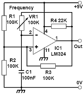
Fig. 4.2.5 Variable Frequency Op-Amp Astable
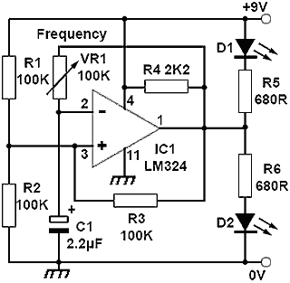
Fig. 4.2.6 Low Frequency LED Flasher
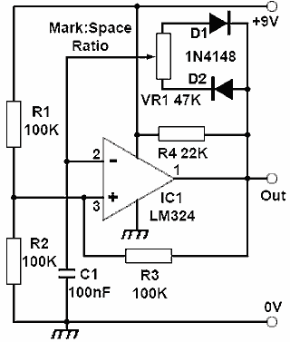
Fig. 4.2.6 Variable Mark to Space Ratio Astable
Modifications to the Basic Astable
Variable Frequency
In Fig. 4.2.5, R5 has been replaced with a 100K variable resistor to make the frequency of oscillation variable. The choice of value for VR1 depends on the frequency range required. An additional fixed resistor could be added in series with VR1 if required to limit the minimum resistance.
Low Frequency LED Flasher
Fig. 4.2.6 shows a low frequency square wave oscillator suitable for driving flashing LEDs. The output of the LM324 is easily capable of providing sufficient current to drive LEDs and this arrangement will source about 10mA to drive D2 when the output is high, and will sink (conduct to ground) the same amount of current when the output is low, to drive D1 from the supply. The frequency may be fixed, using a 33K fixed resistor as in Fig. 4.2.2, or variable using a variable resistor as in Fig. 4.2.6. At low frequencies, a much higher value for C1 is required and therefore an electrolytic capacitor is used. Careful attention must be given to correct polarity when constructing the circuit, and to avoid sudden capacitor failure, a component should be chosen that has a working voltage higher than the supply voltage. However as electrolytic capacitors do not work correctly as capacitors at less than 10% of their rated voltage, the working voltage should ideally not be more than 10 times the supply voltage.
Varying the Mark to space Ratio
Fig. 4.2.7 illustrates a method of generating variable width pulses without affecting the frequency. In this circuit a mark to space ratio control (VR1) and two opposing polarity diodes D1 and D2 form the resistive part of the CR time constant. With VR1 wiper at a central position, a 1:1 mark to space ratio is obtained. When IC1 pin 1 is high, D2 conducts making the lower half of VR1 the active resistor in the CR time constant. When IC1 pin 1 is low, D1 conducts and the upper portion of VR1 is used in the CR time constant. Varying VR1 wiper will provide differing values of resistance during the on and off periods of the waveform, effectively providing either positive going or negative going 9Vpp pulses at the output that can be used for many purposes including PWM (pulse width modulation) for lighting or motor control.


